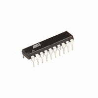
ATTINY2313-20PJ Atmel, ATTINY2313-20PJ Datasheet - Page 54

ATTINY2313-20PJ
Manufacturer Part Number
ATTINY2313-20PJ
Description
IC MCU AVR 2K FLASH 20DIP
Manufacturer
Atmel
Series
AVR® ATtinyr
Specifications of ATTINY2313-20PJ
Core Processor
AVR
Core Size
8-Bit
Speed
20MHz
Connectivity
SPI, UART/USART
Peripherals
Brown-out Detect/Reset, POR, PWM, WDT
Number Of I /o
18
Program Memory Size
2KB (1K x 16)
Program Memory Type
FLASH
Eeprom Size
128 x 8
Ram Size
128 x 8
Voltage - Supply (vcc/vdd)
2.7 V ~ 5.5 V
Oscillator Type
Internal
Operating Temperature
-40°C ~ 85°C
Package / Case
20-DIP (0.300", 7.62mm)
Lead Free Status / RoHS Status
Lead free / RoHS Compliant
Data Converters
-
Other names
ATTINY2313-24PJ
ATTINY2313-24PJ
ATTINY2313-24PJ
- Current page: 54 of 226
- Download datasheet (4Mb)
• DI/SDA/PCINT5 - Port B, Bit 5
DI: Three-wire mode Universal Serial Interface Data input. Three-wire mode does not override
normal port functions, so pin must be configured as an input. SDA: Two-wire mode Serial Inter-
face Data.
PCINT5: Pin Change Interrupt Source 5. The PB5 pin can serve as an external interrupt source.
• OC1B/PCINT4 – Port B, Bit 4
OC1B: Output Compare Match B output: The PB4 pin can serve as an external output for the
Timer/Counter1 Output Compare B. The pin has to be configured as an output (DDB4 set (one))
to serve this function. The OC1B pin is also the output pin for the PWM mode timer function.
PCINT4: Pin Change Interrupt Source 4. The PB4 pin can serve as an external interrupt source.
• OC1A/PCINT3 – Port B, Bit 3
OC1A: Output Compare Match A output: The PB3 pin can serve as an external output for the
Timer/Counter1 Output Compare A. The pin has to be configured as an output (DDB3 set (one))
to serve this function. The OC1A pin is also the output pin for the PWM mode timer function.
PCINT3: Pin Change Interrupt Source 3: The PB3 pin can serve as an external interrupt source.
• OC0A/PCINT2 – Port B, Bit 2
OC0A: Output Compare Match A output. The PB2 pin can serve as an external output for the
Timer/Counter0 Output Compare A. The pin has to be configured as an output (DDB2 set (one))
to serve this function. The OC0A pin is also the output pin for the PWM mode timer function.
PCINT2: Pin Change Interrupt Source 2. The PB2 pin can serve as an external interrupt source.
• AIN1/PCINT1 – Port B, Bit 1
AIN1: Analog Comparator Negative input
Configure the port pin as input with the internal pull-up
.
switched off to avoid the digital port function from interfering with the function of the analog
comparator.
PCINT1: Pin Change Interrupt Source 1. The PB1 pin can serve as an external interrupt source.
• AIN0/PCINT0 – Port B, Bit 0
AIN0: Analog Comparator Positive input. Configure the port pin as input with the internal pull-up
switched off to avoid the digital port function from interfering with the function of the Analog
Comparator.
PCINT0: Pin Change Interrupt Source 0. The PB0 pin can serve as an external interrupt source.
Table 26
and
Table 27
relate the alternate functions of Port B to the overriding signals shown in
Figure 25 on page
51. SPI MSTR INPUT and SPI SLAVE OUTPUT constitute the MISO signal,
while MOSI is divided into SPI MSTR OUTPUT and SPI SLAVE INPUT.
ATtiny2313
54
2543L–AVR–08/10
Related parts for ATTINY2313-20PJ
Image
Part Number
Description
Manufacturer
Datasheet
Request
R

Part Number:
Description:
IC, MCU, 8BIT, 2K FLASH, 20SOIC
Manufacturer:
Atmel
Datasheet:

Part Number:
Description:
IC, MCU, 8BIT, 2K FLASH, 20PDIP
Manufacturer:
Atmel
Datasheet:

Part Number:
Description:
IC, MCU, 8BIT, 8K FLASH, 20PDIP
Manufacturer:
Atmel
Datasheet:

Part Number:
Description:
IC, MCU, 8BIT, 8K FLASH, 20SOIC
Manufacturer:
Atmel
Datasheet:

Part Number:
Description:
DEV KIT FOR AVR/AVR32
Manufacturer:
Atmel
Datasheet:

Part Number:
Description:
INTERVAL AND WIPE/WASH WIPER CONTROL IC WITH DELAY
Manufacturer:
ATMEL Corporation
Datasheet:

Part Number:
Description:
Low-Voltage Voice-Switched IC for Hands-Free Operation
Manufacturer:
ATMEL Corporation
Datasheet:

Part Number:
Description:
MONOLITHIC INTEGRATED FEATUREPHONE CIRCUIT
Manufacturer:
ATMEL Corporation
Datasheet:

Part Number:
Description:
AM-FM Receiver IC U4255BM-M
Manufacturer:
ATMEL Corporation
Datasheet:

Part Number:
Description:
Monolithic Integrated Feature Phone Circuit
Manufacturer:
ATMEL Corporation
Datasheet:

Part Number:
Description:
Multistandard Video-IF and Quasi Parallel Sound Processing
Manufacturer:
ATMEL Corporation
Datasheet:

Part Number:
Description:
High-performance EE PLD
Manufacturer:
ATMEL Corporation
Datasheet:


