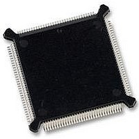
MC68331CEH25 Freescale Semiconductor, MC68331CEH25 Datasheet - Page 27

MC68331CEH25
Manufacturer Part Number
MC68331CEH25
Description
IC MCU 32BIT 25MHZ 132-PQFP
Manufacturer
Freescale Semiconductor
Series
M683xxr
Specifications of MC68331CEH25
Core Processor
CPU32
Core Size
32-Bit
Speed
25MHz
Connectivity
EBI/EMI, SCI, SPI, UART/USART
Peripherals
POR, PWM, WDT
Number Of I /o
18
Program Memory Type
ROMless
Voltage - Supply (vcc/vdd)
4.5 V ~ 5.5 V
Oscillator Type
Internal
Operating Temperature
-40°C ~ 85°C
Package / Case
132-QFP
Controller Family/series
68K
No. Of I/o's
18
Cpu Speed
25MHz
No. Of Timers
1
Embedded Interface Type
QSPI, SCI, UART
No. Of Pwm Channels
2
Digital Ic Case Style
PQFP
Rohs Compliant
Yes
Processor Series
M683xx
Core
CPU32
Data Bus Width
32 bit
Data Ram Size
80 B
Interface Type
QSPI, SCI, UART
Maximum Clock Frequency
25 MHz
Number Of Programmable I/os
18
Number Of Timers
1
Maximum Operating Temperature
+ 85 C
Mounting Style
SMD/SMT
Minimum Operating Temperature
- 40 C
Eeprom Size
-
Ram Size
-
Program Memory Size
-
Data Converters
-
Lead Free Status / Rohs Status
Details
Available stocks
Company
Part Number
Manufacturer
Quantity
Price
Company:
Part Number:
MC68331CEH25
Manufacturer:
PANASONIC
Quantity:
2 000
Company:
Part Number:
MC68331CEH25
Manufacturer:
Freescale Semiconductor
Quantity:
135
Company:
Part Number:
MC68331CEH25
Manufacturer:
Freescale Semiconductor
Quantity:
10 000
3.4.10 Operand Alignment
3.4.11 Misaligned Operands
3.4.12 Operand Transfer Cases
MC68331TS/D
For example, if the MCU is executing an instruction that reads a long-word operand from a 16-bit port,
the MCU latches the 16 bits of valid data and then runs another bus cycle to obtain the other 16 bits.
The operation for an 8-bit port is similar, but requires four read cycles. The addressed device uses the
DSACK0 and DSACK1 signals to indicate the port width. For instance, a 16-bit device always returns
DSACK0 = 1 and DSACK1 = 0 for a 16-bit port, regardless of whether the bus cycle is a byte or word
operation.
Dynamic bus sizing requires that the portion of the data bus used for a transfer to or from a particular
port size be fixed. A 16-bit port must reside on data bus bits [15:0] and an 8-bit port must reside on data
bus bits [15:8]. This minimizes the number of bus cycles needed to transfer data and ensures that the
MCU transfers valid data.
The MCU always attempts to transfer the maximum amount of data on all bus cycles. For a word oper-
ation, it is assumed that the port is 16 bits wide when the bus cycle begins. Operand bytes are desig-
nated as shown in the following figure. OP0 is the most significant byte of a long-word operand, and
OP3 is the least significant byte. The two bytes of a word-length operand are OP0 (most significant) and
OP1. The single byte of a byte-length operand is OP0.
The data multiplexer establishes the necessary connections for different combinations of address and
data sizes. The multiplexer takes the two bytes of the 16-bit bus and routes them to their required po-
sitions. Positioning of bytes is determined by the size and address outputs. SIZ1 and SIZ0 indicate the
remaining number of bytes to be transferred during the current bus cycle. The number of bytes trans-
ferred is equal to or less than the size indicated by SIZ1 and SIZ0, depending on port width.
ADDR0 also affects the operation of the data multiplexer. During an operand transfer, ADDR[23:1] in-
dicate the word base address of the portion of the operand to be accessed, and ADDR0 indicates the
byte offset from the base.
CPU32 processor architecture uses a basic operand size of 16 bits. An operand is misaligned when it
overlaps a word boundary. This is determined by the value of ADDR0. When ADDR0 = 0 (an even ad-
dress), the address is on a word and byte boundary. When ADDR0 = 1 (an odd address), the address
is on a byte boundary only. A byte operand is aligned at any address; a word or long-word operand is
misaligned at an odd address. MC68300 devices do not support misaligned operand transfers.
The largest amount of data that can be transferred by a single bus cycle is an aligned word. If the MCU
transfers a long-word operand via a 16-bit port, the most significant operand word is transferred on the
first bus cycle and the least significant operand word on a following bus cycle.
The following table summarizes how operands are aligned for various types of transfers. OPn entries
are portions of a requested operand that are read or written during a bus cycle and are defined by SIZ1,
SIZ0, and ADDR0 for that bus cycle.
Long Word
Three Byte
Operand
Word
Byte
Freescale Semiconductor, Inc.
For More Information On This Product,
Figure 8 Operand Byte Order
Go to: www.freescale.com
31
OP0
24
23
OP1
OP0
Byte Order
16
15
OP2
OP1
OP0
8
7
OP3
OP2
OP1
OP0
0
27


