MC9S12C96CFUE Freescale Semiconductor, MC9S12C96CFUE Datasheet - Page 336
MC9S12C96CFUE
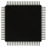
Manufacturer Part Number
MC9S12C96CFUE
Description
IC MCU 96K FLASH 4K RAM 80-QFP
Manufacturer
Freescale Semiconductor
Series
HCS12r
Specifications of MC9S12C96CFUE
Core Processor
HCS12
Core Size
16-Bit
Speed
25MHz
Connectivity
CAN, EBI/EMI, SCI, SPI
Peripherals
POR, PWM, WDT
Number Of I /o
60
Program Memory Size
96KB (96K x 8)
Program Memory Type
FLASH
Ram Size
4K x 8
Voltage - Supply (vcc/vdd)
2.35 V ~ 5.5 V
Data Converters
A/D 8x10b
Oscillator Type
Internal
Operating Temperature
-40°C ~ 85°C
Package / Case
80-QFP
Processor Series
S12C
Core
HCS12
Data Bus Width
16 bit
Data Ram Size
4 KB
Interface Type
CAN/SCI/SPI
Maximum Clock Frequency
25 MHz
Number Of Programmable I/os
60
Number Of Timers
8
Operating Supply Voltage
- 0.3 V to + 6.5 V
Maximum Operating Temperature
+ 85 C
Mounting Style
SMD/SMT
3rd Party Development Tools
EWHCS12
Development Tools By Supplier
M68EVB912C32EE
Minimum Operating Temperature
- 40 C
On-chip Adc
8-ch x 10-bit
Lead Free Status / RoHS Status
Lead free / RoHS Compliant
Eeprom Size
-
Lead Free Status / Rohs Status
Lead free / RoHS Compliant
Available stocks
Company
Part Number
Manufacturer
Quantity
Price

Company:
Part Number:
MC9S12C96CFUE
Manufacturer:
Freescale Semiconductor
Quantity:
10 000
Company:
Part Number:
MC9S12C96CFUER
Manufacturer:
Freescale Semiconductor
Quantity:
10 000


Chapter 10 Freescale’s Scalable Controller Area Network (S12MSCANV2)
If sleep mode is active, the SLPRQ and SLPAK bits are set
use SLPAK as a handshake indication for the request (SLPRQ) to go into sleep mode.
When in sleep mode (SLPRQ = 1 and SLPAK = 1), the MSCAN stops its internal clocks. However, clocks
that allow register accesses from the CPU side continue to run.
If the MSCAN is in bus-off state, it stops counting the 128 occurrences of 11 consecutive recessive bits
due to the stopped clocks. The TXCAN pin remains in a recessive state. If RXF = 1, the message can be
read and RXF can be cleared. Shifting a new message into the foreground buffer of the receiver FIFO
(RxFG) does not take place while in sleep mode.
It is possible to access the transmit buffers and to clear the associated TXE flags. No message abort takes
place while in sleep mode.
If the WUPE bit in CANCLT0 is not asserted, the MSCAN will mask any activity it detects on CAN. The
RXCAN pin is therefore held internally in a recessive state. This locks the MSCAN in sleep mode
(Figure
336
•
•
•
If there are one or more message buffers scheduled for transmission (TXEx = 0), the MSCAN will
continue to transmit until all transmit message buffers are empty (TXEx = 1, transmitted
successfully or aborted) and then goes into sleep mode.
If the MSCAN is receiving, it continues to receive and goes into sleep mode as soon as the CAN
bus next becomes idle.
If the MSCAN is neither transmitting nor receiving, it immediately goes into sleep mode.
10-45). WUPE must be set before entering sleep mode to take effect.
The application software must avoid setting up a transmission (by clearing
one or more TXEx flag(s)) and immediately request sleep mode (by setting
SLPRQ). Whether the MSCAN starts transmitting or goes into sleep mode
directly depends on the exact sequence of operations.
Bus Clock Domain
CPU
Sleep Request
SLPAK
Flag
Figure 10-44. Sleep Request / Acknowledge Cycle
SLPRQ
sync.
SLPAK
MC9S12C-Family / MC9S12GC-Family
Rev 01.24
NOTE
SYNC
SYNC
CAN Clock Domain
(Figure
sync.
SLPRQ
SLPAK
10-44). The application software must
MSCAN
in Sleep Mode
SLPRQ
Flag
Freescale Semiconductor
Related parts for MC9S12C96CFUE
Image
Part Number
Description
Manufacturer
Datasheet
Request
R

Part Number:
Description:
Manufacturer:
Freescale Semiconductor, Inc
Datasheet:
Part Number:
Description:
Manufacturer:
Freescale Semiconductor, Inc
Datasheet:
Part Number:
Description:
Manufacturer:
Freescale Semiconductor, Inc
Datasheet:
Part Number:
Description:
Manufacturer:
Freescale Semiconductor, Inc
Datasheet:
Part Number:
Description:
Manufacturer:
Freescale Semiconductor, Inc
Datasheet:
Part Number:
Description:
Manufacturer:
Freescale Semiconductor, Inc
Datasheet:
Part Number:
Description:
Manufacturer:
Freescale Semiconductor, Inc
Datasheet:
Part Number:
Description:
Manufacturer:
Freescale Semiconductor, Inc
Datasheet:
Part Number:
Description:
Manufacturer:
Freescale Semiconductor, Inc
Datasheet:
Part Number:
Description:
Manufacturer:
Freescale Semiconductor, Inc
Datasheet:
Part Number:
Description:
Manufacturer:
Freescale Semiconductor, Inc
Datasheet:
Part Number:
Description:
Manufacturer:
Freescale Semiconductor, Inc
Datasheet:
Part Number:
Description:
Manufacturer:
Freescale Semiconductor, Inc
Datasheet:
Part Number:
Description:
Manufacturer:
Freescale Semiconductor, Inc
Datasheet:
Part Number:
Description:
Manufacturer:
Freescale Semiconductor, Inc
Datasheet: