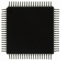
MC9S12C96CFUE Freescale Semiconductor, MC9S12C96CFUE Datasheet - Page 106

MC9S12C96CFUE
Manufacturer Part Number
MC9S12C96CFUE
Description
IC MCU 96K FLASH 4K RAM 80-QFP
Manufacturer
Freescale Semiconductor
Series
HCS12r
Specifications of MC9S12C96CFUE
Core Processor
HCS12
Core Size
16-Bit
Speed
25MHz
Connectivity
CAN, EBI/EMI, SCI, SPI
Peripherals
POR, PWM, WDT
Number Of I /o
60
Program Memory Size
96KB (96K x 8)
Program Memory Type
FLASH
Ram Size
4K x 8
Voltage - Supply (vcc/vdd)
2.35 V ~ 5.5 V
Data Converters
A/D 8x10b
Oscillator Type
Internal
Operating Temperature
-40°C ~ 85°C
Package / Case
80-QFP
Processor Series
S12C
Core
HCS12
Data Bus Width
16 bit
Data Ram Size
4 KB
Interface Type
CAN/SCI/SPI
Maximum Clock Frequency
25 MHz
Number Of Programmable I/os
60
Number Of Timers
8
Operating Supply Voltage
- 0.3 V to + 6.5 V
Maximum Operating Temperature
+ 85 C
Mounting Style
SMD/SMT
3rd Party Development Tools
EWHCS12
Development Tools By Supplier
M68EVB912C32EE
Minimum Operating Temperature
- 40 C
On-chip Adc
8-ch x 10-bit
Lead Free Status / RoHS Status
Lead free / RoHS Compliant
Eeprom Size
-
Lead Free Status / Rohs Status
Lead free / RoHS Compliant
Available stocks
Company
Part Number
Manufacturer
Quantity
Price
Company:
Part Number:
MC9S12C96CFUE
Manufacturer:
Freescale Semiconductor
Quantity:
10 000
Company:
Part Number:
MC9S12C96CFUER
Manufacturer:
Freescale Semiconductor
Quantity:
10 000
- Current page: 106 of 690
- Download datasheet (4Mb)
Chapter 2 Port Integration Module (PIM9C32) Block Description
2.4.2.5
The PWM module is connected to port P. Port P pins can be used as PWM outputs. Further the Keypad
Wake-Up function is implemented on pins PP[7:0]. During reset, port P pins are configured as high-
impedance inputs.
Port P offers 8 general purpose I/O pins with edge triggered interrupt capability in wired-or fashion. The
interrupt enable as well as the sensitivity to rising or falling edges can be individually configured on per
pin basis. All 8 bits/pins share the same interrupt vector. Interrupts can be used with the pins configured
as inputs or outputs.
An interrupt is generated when a bit in the port interrupt flag register and its corresponding port interrupt
enable bit are both set. This external interrupt feature is capable to wake up the CPU when it is in STOP
or WAIT mode.
A digital filter on each pin prevents pulses
interrupt. The minimum time varies over process conditions, temperature and voltage
Table
106
2-38).
Port P
1. These values include the spread of the oscillator frequency over temperature,
Glitch, filtered out, no interrupt flag set
Valid pulse, interrupt flag set
voltage and process.
Uncertain
Ignored
Pulse
Figure 2-47. Interrupt Glitch Filter on Port P and J (PPS = 0)
Valid
Table 2-38. Pulse Detection Criteria
3 < t
MC9S12C-Family / MC9S12GC-Family
t
t
pign
Figure 2-48. Pulse Illustration
pval
t
Value
pign
pulse
<= 3
>= 4
STOP Mode
(Figure
t
pval
< 4
Rev 01.24
t
pulse
2-48) shorter than a specified time from generating an
Bus clocks
Bus clocks
Bus clocks
Unit
3.2 < t
t
pign
t
pval
STOP
Value
pulse
<= 3.2
>= 10
(1)
< 10
Mode
Unit
µs
µs
µs
Freescale Semiconductor
(Figure 2-47
and
Related parts for MC9S12C96CFUE
Image
Part Number
Description
Manufacturer
Datasheet
Request
R
Part Number:
Description:
Manufacturer:
Freescale Semiconductor, Inc
Datasheet:
Part Number:
Description:
Manufacturer:
Freescale Semiconductor, Inc
Datasheet:
Part Number:
Description:
Manufacturer:
Freescale Semiconductor, Inc
Datasheet:
Part Number:
Description:
Manufacturer:
Freescale Semiconductor, Inc
Datasheet:
Part Number:
Description:
Manufacturer:
Freescale Semiconductor, Inc
Datasheet:
Part Number:
Description:
Manufacturer:
Freescale Semiconductor, Inc
Datasheet:
Part Number:
Description:
Manufacturer:
Freescale Semiconductor, Inc
Datasheet:
Part Number:
Description:
Manufacturer:
Freescale Semiconductor, Inc
Datasheet:
Part Number:
Description:
Manufacturer:
Freescale Semiconductor, Inc
Datasheet:
Part Number:
Description:
Manufacturer:
Freescale Semiconductor, Inc
Datasheet:
Part Number:
Description:
Manufacturer:
Freescale Semiconductor, Inc
Datasheet:
Part Number:
Description:
Manufacturer:
Freescale Semiconductor, Inc
Datasheet:
Part Number:
Description:
Manufacturer:
Freescale Semiconductor, Inc
Datasheet:
Part Number:
Description:
Manufacturer:
Freescale Semiconductor, Inc
Datasheet:
Part Number:
Description:
Manufacturer:
Freescale Semiconductor, Inc
Datasheet:


