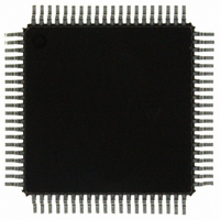
MC9S12C96CFUE Freescale Semiconductor, MC9S12C96CFUE Datasheet - Page 107

MC9S12C96CFUE
Manufacturer Part Number
MC9S12C96CFUE
Description
IC MCU 96K FLASH 4K RAM 80-QFP
Manufacturer
Freescale Semiconductor
Series
HCS12r
Specifications of MC9S12C96CFUE
Core Processor
HCS12
Core Size
16-Bit
Speed
25MHz
Connectivity
CAN, EBI/EMI, SCI, SPI
Peripherals
POR, PWM, WDT
Number Of I /o
60
Program Memory Size
96KB (96K x 8)
Program Memory Type
FLASH
Ram Size
4K x 8
Voltage - Supply (vcc/vdd)
2.35 V ~ 5.5 V
Data Converters
A/D 8x10b
Oscillator Type
Internal
Operating Temperature
-40°C ~ 85°C
Package / Case
80-QFP
Processor Series
S12C
Core
HCS12
Data Bus Width
16 bit
Data Ram Size
4 KB
Interface Type
CAN/SCI/SPI
Maximum Clock Frequency
25 MHz
Number Of Programmable I/os
60
Number Of Timers
8
Operating Supply Voltage
- 0.3 V to + 6.5 V
Maximum Operating Temperature
+ 85 C
Mounting Style
SMD/SMT
3rd Party Development Tools
EWHCS12
Development Tools By Supplier
M68EVB912C32EE
Minimum Operating Temperature
- 40 C
On-chip Adc
8-ch x 10-bit
Lead Free Status / RoHS Status
Lead free / RoHS Compliant
Eeprom Size
-
Lead Free Status / Rohs Status
Lead free / RoHS Compliant
Available stocks
Company
Part Number
Manufacturer
Quantity
Price
Company:
Part Number:
MC9S12C96CFUE
Manufacturer:
Freescale Semiconductor
Quantity:
10 000
Company:
Part Number:
MC9S12C96CFUER
Manufacturer:
Freescale Semiconductor
Quantity:
10 000
- Current page: 107 of 690
- Download datasheet (4Mb)
A valid edge on input is detected if 4 consecutive samples of a passive level are followed by 4 consecutive
samples of an active level directly or indirectly.
The filters are continuously clocked by the bus clock in RUN and WAIT mode. In STOP mode the clock
is generated by a single RC oscillator in the Port Integration Module. To maximize current saving the RC
oscillator runs only if the following condition is true on any pin:
Sample count <= 4 and port interrupt enabled (PIE=1) and port interrupt flag not set (PIF=0).
2.4.2.6
In all modes, port J pins PJ[7:6] can be used for general purpose I/O or interrupt driven general purpose
I/O’s. During reset, port J pins are configured as inputs.
Port J offers 2 I/O ports with the same interrupt features as on port P.
2.4.3
All port and pin logic is located in the core module. Please refer to S12_mebi Block User Guide for details.
2.4.4
All ports start up as general purpose inputs on reset.
2.4.5
2.4.5.1
No low power options exist for this module in run mode.
2.4.5.2
No low power options exist for this module in wait mode.
2.4.5.3
All clocks are stopped. There are asynchronous paths to generate interrupts from STOP on port P and J.
2.5
The reset values of all registers are given in
2.5.1
All registers including the data registers get set/reset asynchronously.
properties after reset initialization.
Freescale Semiconductor
Initialization Information
Port A, B, E and BKGD Pin
External Pin Descriptions
Low Power Options
Reset Initialization
Port J
Run Mode
Wait Mode
Stop Mode
MC9S12C-Family / MC9S12GC-Family
Section 2.3.2, “Register
Rev 01.24
Chapter 2 Port Integration Module (PIM9C32) Block Description
Descriptions”.
Table 2-39
summarizes the port
107
Related parts for MC9S12C96CFUE
Image
Part Number
Description
Manufacturer
Datasheet
Request
R
Part Number:
Description:
Manufacturer:
Freescale Semiconductor, Inc
Datasheet:
Part Number:
Description:
Manufacturer:
Freescale Semiconductor, Inc
Datasheet:
Part Number:
Description:
Manufacturer:
Freescale Semiconductor, Inc
Datasheet:
Part Number:
Description:
Manufacturer:
Freescale Semiconductor, Inc
Datasheet:
Part Number:
Description:
Manufacturer:
Freescale Semiconductor, Inc
Datasheet:
Part Number:
Description:
Manufacturer:
Freescale Semiconductor, Inc
Datasheet:
Part Number:
Description:
Manufacturer:
Freescale Semiconductor, Inc
Datasheet:
Part Number:
Description:
Manufacturer:
Freescale Semiconductor, Inc
Datasheet:
Part Number:
Description:
Manufacturer:
Freescale Semiconductor, Inc
Datasheet:
Part Number:
Description:
Manufacturer:
Freescale Semiconductor, Inc
Datasheet:
Part Number:
Description:
Manufacturer:
Freescale Semiconductor, Inc
Datasheet:
Part Number:
Description:
Manufacturer:
Freescale Semiconductor, Inc
Datasheet:
Part Number:
Description:
Manufacturer:
Freescale Semiconductor, Inc
Datasheet:
Part Number:
Description:
Manufacturer:
Freescale Semiconductor, Inc
Datasheet:
Part Number:
Description:
Manufacturer:
Freescale Semiconductor, Inc
Datasheet:


