Z8F0412SJ020SG Zilog, Z8F0412SJ020SG Datasheet - Page 6
Z8F0412SJ020SG
Manufacturer Part Number
Z8F0412SJ020SG
Description
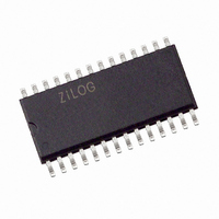
IC ENCORE MCU FLASH 4K 28SOIC
Manufacturer
Zilog
Series
Encore!® XP®r
Datasheet
1.Z8F08200100KIT.pdf
(264 pages)
Specifications of Z8F0412SJ020SG
Core Processor
Z8
Core Size
8-Bit
Speed
20MHz
Connectivity
I²C, IrDA, SPI, UART/USART
Peripherals
Brown-out Detect/Reset, POR, PWM, WDT
Number Of I /o
19
Program Memory Size
4KB (4K x 8)
Program Memory Type
FLASH
Ram Size
1K x 8
Voltage - Supply (vcc/vdd)
2.7 V ~ 3.6 V
Oscillator Type
Internal
Operating Temperature
0°C ~ 70°C
Package / Case
28-SOIC (7.5mm Width)
Processor Series
Z8F041xx
Core
eZ8
Data Bus Width
8 bit
Data Ram Size
1 KB
Interface Type
I2C, SPI, UART
Maximum Clock Frequency
20 MHz
Number Of Programmable I/os
19
Number Of Timers
2
Operating Supply Voltage
2.7 V to 3.6 V
Maximum Operating Temperature
+ 70 C
Mounting Style
SMD/SMT
Minimum Operating Temperature
0 C
Lead Free Status / RoHS Status
Lead free / RoHS Compliant
Eeprom Size
-
Data Converters
-
Lead Free Status / Rohs Status
Details
Other names
269-4107
Z8F0412SJ020SG
Z8F0412SJ020SG
Available stocks
Company
Part Number
Manufacturer
Quantity
Price

Part Number:
Z8F0412SJ020SG
Manufacturer:
ZILOG
Quantity:
20 000


PS022517-0508
Watchdog Timer . . . . . . . . . . . . . . . . . . . . . . . . . . . . . . . . . . . . . . . . . . . . . . . . . . . 83
Universal Asynchronous Receiver/Transmitter . . . . . . . . . . . . . . . . . . . . . . . . . 89
Infrared Encoder/Decoder . . . . . . . . . . . . . . . . . . . . . . . . . . . . . . . . . . . . . . . . . . 109
Operation . . . . . . . . . . . . . . . . . . . . . . . . . . . . . . . . . . . . . . . . . . . . . . . . . . . . . . 69
Timer Control Register Definitions . . . . . . . . . . . . . . . . . . . . . . . . . . . . . . . . . . . 78
Operation . . . . . . . . . . . . . . . . . . . . . . . . . . . . . . . . . . . . . . . . . . . . . . . . . . . . . . 83
Watchdog Timer Control Register Definitions . . . . . . . . . . . . . . . . . . . . . . . . . . 86
Architecture . . . . . . . . . . . . . . . . . . . . . . . . . . . . . . . . . . . . . . . . . . . . . . . . . . . . 89
Operation . . . . . . . . . . . . . . . . . . . . . . . . . . . . . . . . . . . . . . . . . . . . . . . . . . . . . . 90
UART Control Register Definitions. . . . . . . . . . . . . . . . . . . . . . . . . . . . . . . . . . 100
Architecture . . . . . . . . . . . . . . . . . . . . . . . . . . . . . . . . . . . . . . . . . . . . . . . . . . . 109
Timer Operating Modes . . . . . . . . . . . . . . . . . . . . . . . . . . . . . . . . . . . . . . . . 70
Reading the Timer Count Values . . . . . . . . . . . . . . . . . . . . . . . . . . . . . . . . . 77
Timer Output Signal Operation. . . . . . . . . . . . . . . . . . . . . . . . . . . . . . . . . . . 78
Timer 0–1 High and Low Byte Registers . . . . . . . . . . . . . . . . . . . . . . . . . . . 78
Timer Reload High and Low Byte Registers . . . . . . . . . . . . . . . . . . . . . . . . 79
Timer 0–1 PWM High and Low Byte Registers . . . . . . . . . . . . . . . . . . . . . . 79
Timer 0–3 Control 0 Registers . . . . . . . . . . . . . . . . . . . . . . . . . . . . . . . . . . . 80
Timer 0–1 Control 1 Registers . . . . . . . . . . . . . . . . . . . . . . . . . . . . . . . . . . . 81
Watchdog Timer Refresh . . . . . . . . . . . . . . . . . . . . . . . . . . . . . . . . . . . . . . . 84
Watchdog Timer Time-Out Response . . . . . . . . . . . . . . . . . . . . . . . . . . . . . 84
Watchdog Timer Reload Unlock Sequence . . . . . . . . . . . . . . . . . . . . . . . . . 85
Watchdog Timer Control Register . . . . . . . . . . . . . . . . . . . . . . . . . . . . . . . . 86
Watchdog Timer Reload Upper, High and Low Byte Registers . . . . . . . . . . 87
Data Format . . . . . . . . . . . . . . . . . . . . . . . . . . . . . . . . . . . . . . . . . . . . . . . . . 90
Transmitting Data using Polled Method . . . . . . . . . . . . . . . . . . . . . . . . . . . . 91
Transmitting Data Using Interrupt-Driven Method . . . . . . . . . . . . . . . . . . . . 92
Receiving Data using the Polled Method . . . . . . . . . . . . . . . . . . . . . . . . . . . 93
Receiving Data Using Interrupt-Driven Method . . . . . . . . . . . . . . . . . . . . . . 94
Clear To Send Operation . . . . . . . . . . . . . . . . . . . . . . . . . . . . . . . . . . . . . . . 95
Multiprocessor (9-bit) Mode . . . . . . . . . . . . . . . . . . . . . . . . . . . . . . . . . . . . . 95
External Driver Enable . . . . . . . . . . . . . . . . . . . . . . . . . . . . . . . . . . . . . . . . . 96
UART Interrupts . . . . . . . . . . . . . . . . . . . . . . . . . . . . . . . . . . . . . . . . . . . . . . 97
UART Transmit Data Register . . . . . . . . . . . . . . . . . . . . . . . . . . . . . . . . . . 100
UART Receive Data Register. . . . . . . . . . . . . . . . . . . . . . . . . . . . . . . . . . . 101
UART Status 0 Register . . . . . . . . . . . . . . . . . . . . . . . . . . . . . . . . . . . . . . . 101
UART Status 1 Register . . . . . . . . . . . . . . . . . . . . . . . . . . . . . . . . . . . . . . . 102
UART Control 0 and Control 1 Registers . . . . . . . . . . . . . . . . . . . . . . . . . . 103
UART Address Compare Register . . . . . . . . . . . . . . . . . . . . . . . . . . . . . . . 105
UART Baud Rate High and Low Byte Registers . . . . . . . . . . . . . . . . . . . . 106
UART Baud Rate Generator . . . . . . . . . . . . . . . . . . . . . . . . . . . . . . . . . . . . 99
Z8 Encore! XP
Product Specification
®
Table of Contents
F0822 Series
vi
Related parts for Z8F0412SJ020SG
Image
Part Number
Description
Manufacturer
Datasheet
Request
R

Part Number:
Description:
Communication Controllers, ZILOG INTELLIGENT PERIPHERAL CONTROLLER (ZIP)
Manufacturer:
Zilog, Inc.
Datasheet:

Part Number:
Description:
KIT DEV FOR Z8 ENCORE 16K TO 64K
Manufacturer:
Zilog
Datasheet:

Part Number:
Description:
KIT DEV Z8 ENCORE XP 28-PIN
Manufacturer:
Zilog
Datasheet:

Part Number:
Description:
DEV KIT FOR Z8 ENCORE 8K/4K
Manufacturer:
Zilog
Datasheet:

Part Number:
Description:
KIT DEV Z8 ENCORE XP 28-PIN
Manufacturer:
Zilog
Datasheet:

Part Number:
Description:
DEV KIT FOR Z8 ENCORE 4K TO 8K
Manufacturer:
Zilog
Datasheet:
Part Number:
Description:
CMOS Z8 microcontroller. ROM 16 Kbytes, RAM 256 bytes, speed 16 MHz, 32 lines I/O, 3.0V to 5.5V
Manufacturer:
Zilog, Inc.
Datasheet:
Part Number:
Description:
Low-cost microcontroller. 512 bytes ROM, 61 bytes RAM, 8 MHz
Manufacturer:
Zilog, Inc.
Datasheet:
Part Number:
Description:
Z8 4K OTP Microcontroller
Manufacturer:
Zilog, Inc.
Datasheet:
Part Number:
Description:
CMOS SUPER8 ROMLESS MCU
Manufacturer:
Zilog, Inc.
Datasheet:
Part Number:
Description:
SL1866 CMOSZ8 OTP Microcontroller
Manufacturer:
Zilog, Inc.
Datasheet:
Part Number:
Description:
SL1866 CMOSZ8 OTP Microcontroller
Manufacturer:
Zilog, Inc.
Datasheet:
Part Number:
Description:
OTP (KB) = 1, RAM = 125, Speed = 12, I/O = 14, 8-bit Timers = 2, Comm Interfaces Other Features = Por, LV Protect, Voltage = 4.5-5.5V
Manufacturer:
Zilog, Inc.
Datasheet:
Part Number:
Description:
Manufacturer:
Zilog, Inc.
Datasheet: