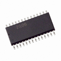
Z8F0412SJ020SG Zilog, Z8F0412SJ020SG Datasheet - Page 169

Z8F0412SJ020SG
Manufacturer Part Number
Z8F0412SJ020SG
Description
IC ENCORE MCU FLASH 4K 28SOIC
Manufacturer
Zilog
Series
Encore!® XP®r
Datasheet
1.Z8F08200100KIT.pdf
(264 pages)
Specifications of Z8F0412SJ020SG
Core Processor
Z8
Core Size
8-Bit
Speed
20MHz
Connectivity
I²C, IrDA, SPI, UART/USART
Peripherals
Brown-out Detect/Reset, POR, PWM, WDT
Number Of I /o
19
Program Memory Size
4KB (4K x 8)
Program Memory Type
FLASH
Ram Size
1K x 8
Voltage - Supply (vcc/vdd)
2.7 V ~ 3.6 V
Oscillator Type
Internal
Operating Temperature
0°C ~ 70°C
Package / Case
28-SOIC (7.5mm Width)
Processor Series
Z8F041xx
Core
eZ8
Data Bus Width
8 bit
Data Ram Size
1 KB
Interface Type
I2C, SPI, UART
Maximum Clock Frequency
20 MHz
Number Of Programmable I/os
19
Number Of Timers
2
Operating Supply Voltage
2.7 V to 3.6 V
Maximum Operating Temperature
+ 70 C
Mounting Style
SMD/SMT
Minimum Operating Temperature
0 C
Lead Free Status / RoHS Status
Lead free / RoHS Compliant
Eeprom Size
-
Data Converters
-
Lead Free Status / Rohs Status
Details
Other names
269-4107
Z8F0412SJ020SG
Z8F0412SJ020SG
Available stocks
Company
Part Number
Manufacturer
Quantity
Price
Part Number:
Z8F0412SJ020SG
Manufacturer:
ZILOG
Quantity:
20 000
- Current page: 169 of 264
- Download datasheet (6Mb)
PS022517-0508
Flash Read Protection
Flash Write/Erase Protection
The user code contained within the Flash memory can be protected from external access.
Programming the Flash Read Protect Option Bit prevents reading of user code by the
OCD or by using the Flash Controller Bypass mode. For more information, see
Bits
Z8 Encore! XP
gram and erasure of the Flash memory contents. This protection is provided by the Flash
Controller unlock mechanism, the Flash Sector Protect Register, and the Flash Write Pro-
tect option bit.
Flash Controller Unlock Mechanism
At Reset, the Flash Controller locks to prevent accidental program or erasure of the Flash
memory. To program or erase the Flash memory, the Flash controller must be unlocked.
After unlocking the Flash Controller, the Flash can be programmed or erased. Any value
written by user code to the Flash Control Register or Page Select Register out of sequence
locks the Flash Controller.
Follow the steps below to unlock the Flash Controller from user code:
1. Write
2. Write the page to be programmed or erased to the Page Select Register.
3. Write the first unlock command
4. Write the second unlock command
5. Re-write the page written in
Flash Sector Protection
The Flash Sector Protect Register is configured to prevent sectors from being programmed
or erased. Once a sector is protected, it cannot be unprotected by user code. The Flash
Sector Protect Register is cleared after reset and any previously written protection values
is lost. User code must write this register in the initialization routine if enable sector
protection is desired.
The Flash Sector Protect Register shares its Register File address with the Page Select
Register. The Flash Sector Protect Register is accessed by writing the Flash Control
Register with
at the Page Select Register address. When the user code writes the Flash Sector Protect
Register, bits can only be set to 1. Sectors can be protected, but not unprotected, using reg-
ister write operations. Writing a value other than
lects the Flash Sector Protect Register and re-enables access to the Page Select Register.
on page 163 and
00H
5EH
®
to the Flash Control Register to reset the Flash Controller.
F0822 Series provides several levels of protection against accidental pro-
. After the Flash Sector Protect Register is selected, it can be accessed
On-Chip Debugger
step 2
73H
to the Page Select Register.
8CH
to the Flash Control Register.
on page 171.
to the Flash Control Register.
5EH
to the Flash Control Register dese-
Z8 Encore! XP
Product Specification
®
F0822 Series
Flash Memory
Option
156
Related parts for Z8F0412SJ020SG
Image
Part Number
Description
Manufacturer
Datasheet
Request
R

Part Number:
Description:
Communication Controllers, ZILOG INTELLIGENT PERIPHERAL CONTROLLER (ZIP)
Manufacturer:
Zilog, Inc.
Datasheet:

Part Number:
Description:
KIT DEV FOR Z8 ENCORE 16K TO 64K
Manufacturer:
Zilog
Datasheet:

Part Number:
Description:
KIT DEV Z8 ENCORE XP 28-PIN
Manufacturer:
Zilog
Datasheet:

Part Number:
Description:
DEV KIT FOR Z8 ENCORE 8K/4K
Manufacturer:
Zilog
Datasheet:

Part Number:
Description:
KIT DEV Z8 ENCORE XP 28-PIN
Manufacturer:
Zilog
Datasheet:

Part Number:
Description:
DEV KIT FOR Z8 ENCORE 4K TO 8K
Manufacturer:
Zilog
Datasheet:

Part Number:
Description:
CMOS Z8 microcontroller. ROM 16 Kbytes, RAM 256 bytes, speed 16 MHz, 32 lines I/O, 3.0V to 5.5V
Manufacturer:
Zilog, Inc.
Datasheet:

Part Number:
Description:
Low-cost microcontroller. 512 bytes ROM, 61 bytes RAM, 8 MHz
Manufacturer:
Zilog, Inc.
Datasheet:

Part Number:
Description:
Z8 4K OTP Microcontroller
Manufacturer:
Zilog, Inc.
Datasheet:

Part Number:
Description:
CMOS SUPER8 ROMLESS MCU
Manufacturer:
Zilog, Inc.
Datasheet:

Part Number:
Description:
SL1866 CMOSZ8 OTP Microcontroller
Manufacturer:
Zilog, Inc.
Datasheet:

Part Number:
Description:
SL1866 CMOSZ8 OTP Microcontroller
Manufacturer:
Zilog, Inc.
Datasheet:

Part Number:
Description:
OTP (KB) = 1, RAM = 125, Speed = 12, I/O = 14, 8-bit Timers = 2, Comm Interfaces Other Features = Por, LV Protect, Voltage = 4.5-5.5V
Manufacturer:
Zilog, Inc.
Datasheet:

Part Number:
Description:
Manufacturer:
Zilog, Inc.
Datasheet:


