ST7FLITES2Y0M6 STMicroelectronics, ST7FLITES2Y0M6 Datasheet - Page 7
ST7FLITES2Y0M6
Manufacturer Part Number
ST7FLITES2Y0M6
Description
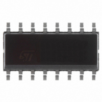
MCU 8BIT 1K FLASH 16SOIC
Manufacturer
STMicroelectronics
Series
ST7r
Datasheet
1.ST7FLITES2Y0B6.pdf
(124 pages)
Specifications of ST7FLITES2Y0M6
Core Processor
ST7
Core Size
8-Bit
Speed
8MHz
Connectivity
SPI
Peripherals
LVD, POR, PWM, WDT
Number Of I /o
13
Program Memory Size
1KB (1K x 8)
Program Memory Type
FLASH
Ram Size
128 x 8
Voltage - Supply (vcc/vdd)
2.4 V ~ 5.5 V
Oscillator Type
Internal
Operating Temperature
-40°C ~ 85°C
Package / Case
16-SOIC (3.9mm Width)
Controller Family/series
ST7
No. Of I/o's
13
Ram Memory Size
128Byte
Cpu Speed
8MHz
No. Of Timers
2
Embedded Interface Type
SPI
No. Of Pwm Channels
1
Rohs Compliant
Yes
Processor Series
ST7FLITESx
Core
ST7
Data Bus Width
8 bit
Data Ram Size
128 B
Interface Type
SPI
Maximum Clock Frequency
8 MHz
Number Of Programmable I/os
13
Number Of Timers
2
Operating Supply Voltage
2.4 V to 5.5 V
Maximum Operating Temperature
+ 85 C
Mounting Style
SMD/SMT
Development Tools By Supplier
ST7FLIT0-IND/USB, ST7FLITE-SK/RAIS, ST7MDT10-DVP3, ST7MDT10-EMU3, STX-RLINK
Minimum Operating Temperature
- 40 C
On-chip Adc
8 bit
For Use With
497-5858 - EVAL BOARD PLAYBACK ST7FLITE497-5049 - KIT STARTER RAISONANCE ST7FLITE
Lead Free Status / RoHS Status
Lead free / RoHS Compliant
Eeprom Size
-
Data Converters
-
Lead Free Status / Rohs Status
In Transition
Other names
497-4861
Available stocks
Company
Part Number
Manufacturer
Quantity
Price


PIN DESCRIPTION (Cont’d)
Legend / Abbreviations for
Type:
In/Output level: C= CMOS 0.15V
Output level:
Port and control configuration:
Table 1. Device Pin Description
– Input:
– Output:
Pin n°
18
19
20
10 10
11 11
12 12 PA4
14 13 PA3
1
6
5
7
8
9
1
2
3
4
5
6
7
8
9
V
V
RESET
PB0/AIN0/SS
PB1/AIN1/SCK
PB2/AIN2/MISO
PB3/AIN3/MOSI
PB4/AIN4/CLKIN
PA7
PA6 /MCO/
ICCCLK
PA5/
ICCDATA
SS
DD
Pin Name
I = input, O = output, S = supply
C
HS = 20mA high sink (on N-buffer only)
float = floating, wpu = weak pull-up, int = interrupt
OD = open drain, PP = push-pull
T
= CMOS 0.3V
I/O
I/O
I/O
I/O
I/O
I/O
I/O
I/O
I/O C
I/O C
I/O C
S
S
Table
Level
T
T
T
C
C
C
C
C
C
C
C
DD
DD
T
T
T
T
T
T
T
T
HS
HS
HS
1:
/0.7V
/0.85V
X
X
X
X
X
X
X
X
X
X
DD
DD
X
X
X
X
X
X
X
X
Port / Control
Input
with input trigger
ei3
ei2
ei1
with input trigger
X
X
X
X
X
Output
X
X
X
X
X
X
X
X
X
X
X
X
X
X
X
X
X
X
X
X
X
(after reset)
Ground
Main power supply
Top priority non maskable interrupt (active low)
Port B0
Port B1
Port B2
Port B3
Port B4
Port A7
Port A6
Port A5
Port A4
Port A3
Function
Main
1)
, ana = analog
ST7LITE0xY0, ST7LITESxY0
ADC Analog Input 0 or SPI Slave
Select (active low)
ADC Analog Input 1 or SPI Clock
Caution: No negative current in-
jection allowed on this pin. For
details, refer to
page 82
ADC Analog Input 2 or SPI Mas-
ter In/ Slave Out Data
ADC Analog Input 3 or SPI Mas-
ter Out / Slave In Data
ADC Analog Input 4 or External
clock input
Main Clock Output/In Circuit
Communication Clock.
Caution: During normal opera-
tion this pin must be pulled- up,
internally or externally (external
pull-up of 10k mandatory in noisy
environment). This is to avoid en-
tering ICC mode unexpectedly
during a reset. In the application,
even if the pin is configured as
output, any reset will put it back in
input pull-up
In Circuit Communication Data
Alternate Function
section 13.2.2 on
7/124
1
Related parts for ST7FLITES2Y0M6
Image
Part Number
Description
Manufacturer
Datasheet
Request
R

Part Number:
Description:
KIT STARTER RAISONANCE ST7FLITE
Manufacturer:
STMicroelectronics
Datasheet:

Part Number:
Description:
STMicroelectronics [RIPPLE-CARRY BINARY COUNTER/DIVIDERS]
Manufacturer:
STMicroelectronics
Datasheet:
Part Number:
Description:
STMicroelectronics [LIQUID-CRYSTAL DISPLAY DRIVERS]
Manufacturer:
STMicroelectronics
Datasheet:

Part Number:
Description:
BOARD EVAL FOR MEMS SENSORS
Manufacturer:
STMicroelectronics
Datasheet:
Part Number:
Description:
NPN TRANSISTOR POWER MODULE
Manufacturer:
STMicroelectronics
Datasheet:
Part Number:
Description:
TURBOSWITCH ULTRA-FAST HIGH VOLTAGE DIODE
Manufacturer:
STMicroelectronics
Datasheet:
Part Number:
Description:
Manufacturer:
STMicroelectronics
Datasheet:
Part Number:
Description:
DIODE / SCR MODULE
Manufacturer:
STMicroelectronics
Datasheet:
Part Number:
Description:
DIODE / SCR MODULE
Manufacturer:
STMicroelectronics
Datasheet:
Part Number:
Description:
Search -----> STE16N100
Manufacturer:
STMicroelectronics
Datasheet:
Part Number:
Description:
Search ---> STE53NA50
Manufacturer:
STMicroelectronics
Datasheet:
Part Number:
Description:
NPN Transistor Power Module
Manufacturer:
STMicroelectronics
Datasheet: