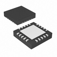
PIC18LF14K22-I/ML Microchip Technology, PIC18LF14K22-I/ML Datasheet - Page 225

PIC18LF14K22-I/ML
Manufacturer Part Number
PIC18LF14K22-I/ML
Description
IC PIC MCU FLASH 512KX16 20-QFN
Manufacturer
Microchip Technology
Series
PIC® XLP™ 18Fr
Datasheets
1.PIC18LF13K22-ISS.pdf
(388 pages)
2.PIC18LF13K22-ISS.pdf
(12 pages)
3.PIC18LF13K22-ISS.pdf
(36 pages)
4.PIC18LF14K22-IP.pdf
(382 pages)
Specifications of PIC18LF14K22-I/ML
Program Memory Type
FLASH
Program Memory Size
16KB (8K x 16)
Package / Case
20-VQFN Exposed Pad, 20-HVQFN, 20-SQFN, 20-DHVQFN
Core Processor
PIC
Core Size
8-Bit
Speed
64MHz
Connectivity
I²C, LIN, SPI, UART/USART
Peripherals
Brown-out Detect/Reset, POR, PWM, WDT
Number Of I /o
17
Eeprom Size
256 x 8
Ram Size
512 x 8
Voltage - Supply (vcc/vdd)
1.8 V ~ 3.6 V
Data Converters
A/D 12x10b
Oscillator Type
Internal
Operating Temperature
-40°C ~ 85°C
Processor Series
PIC18LF
Core
PIC
Data Bus Width
8 bit
Data Ram Size
512 B
Interface Type
I2C, MSSP, SPI, USART
Maximum Clock Frequency
32 KHz
Number Of Programmable I/os
18
Number Of Timers
4
Operating Supply Voltage
1.8 V to 3.6 V
Maximum Operating Temperature
+ 125 C
Mounting Style
SMD/SMT
3rd Party Development Tools
52715-96, 52716-328, 52717-734, 52712-325, EWPIC18
Development Tools By Supplier
PG164130, DV164035, DV244005, DV164005
Minimum Operating Temperature
- 40 C
On-chip Adc
10 bit, 12 Channel
Lead Free Status / RoHS Status
Lead free / RoHS Compliant
Lead Free Status / RoHS Status
Lead free / RoHS Compliant, Lead free / RoHS Compliant
Available stocks
Company
Part Number
Manufacturer
Quantity
Price
Part Number:
PIC18LF14K22-I/ML
Manufacturer:
MICROCHIP/微芯
Quantity:
20 000
- PIC18LF13K22-ISS PDF datasheet
- PIC18LF13K22-ISS PDF datasheet #2
- PIC18LF13K22-ISS PDF datasheet #3
- PIC18LF14K22-IP PDF datasheet #4
- Current page: 225 of 388
- Download datasheet (4Mb)
17.4
The comparator interrupt flag can be set whenever
there is a change in the output value of the comparator.
Changes are recognized by means of a mismatch
circuit which consists of two latches and an exclusive-
or gate (see Figure 17-2 and Figure 17-3). One latch is
updated with the comparator output level when the
CMxCON0 register is read. This latch retains the value
until the next read of the CMxCON0 register or the
occurrence of a Reset. The other latch of the mismatch
circuit is updated on every Q1 system clock. A
mismatch condition will occur when a comparator
output change is clocked through the second latch on
the Q1 clock cycle. At this point the two mismatch
latches have opposite output levels which is detected
by the exclusive-or gate and fed to the interrupt
circuitry. The mismatch condition persists until either
the CMxCON0 register is read or the comparator
output returns to the previous state.
The comparator interrupt is set by the mismatch edge
and not the mismatch level. This means that the inter-
rupt flag can be reset without the additional step of
reading or writing the CMxCON0 register to clear the
mismatch registers. When the mismatch registers are
cleared, an interrupt will occur upon the comparator’s
return to the previous state, otherwise no interrupt will
be generated.
Software will need to maintain information about the
status of the comparator output, as read from the
CMxCON0 register, or CM2CON1 register, to determine
the actual change that has occurred. See Figures 17-4
and 17-5.
The CxIF bit of the PIR2 register is the comparator
interrupt flag. This bit must be reset by software by
clearing it to ‘0’. Since it is also possible to write a ‘1’ to
this register, an interrupt can be generated.
In mid-range Compatibility mode the CxIE bit of the
PIE2 register and the PEIE and GIE bits of the INTCON
register must all be set to enable comparator interrupts.
If any of these bits are cleared, the interrupt is not
enabled, although the CxIF bit of the PIR2 register will
still be set if an interrupt condition occurs.
2010 Microchip Technology Inc.
Note 1: A write operation to the CMxCON0
2: Comparator interrupts will operate correctly
Comparator Interrupt Operation
register will also clear the mismatch
condition because all writes include a read
operation at the beginning of the write
cycle.
regardless of the state of CxOE.
Preliminary
PIC18F1XK22/LF1XK22
17.4.1
The comparator mismatch latches can be preset to the
desired state before the comparators are enabled.
When the comparator is off the CxPOL bit controls the
CxOUT level. Set the CxPOL bit to the desired CxOUT
non-interrupt level while the CxON bit is cleared. Then,
configure the desired CxPOL level in the same instruc-
tion that the CxON bit is set. Since all register writes are
performed as a Read-Modify-Write, the mismatch
latches will be cleared during the instruction Read
phase and the actual configuration of the CxON and
CxPOL bits will be occur in the final Write phase.
FIGURE 17-4:
FIGURE 17-5:
Q1
Q3
CxIN+
CxIN
Set CxIF (edge)
CxIF
Q1
Q3
CxIN+
CxOUT
Set CxIF (edge)
CxIF
Note 1: If a change in the CMxCON0 register
Cleared by CMxCON0 Read
2: When either comparator is first enabled,
PRESETTING THE MISMATCH
LATCHES
(CxOUT) should occur when a read oper-
ation is being executed (start of the Q2
cycle), then the CxIF interrupt flag of the
PIR2 register may not get set.
bias circuitry in the comparator module
may cause an invalid output from the
comparator until the bias circuitry is stable.
Allow about 1 s for bias settling then clear
the mismatch condition and interrupt flags
before enabling comparator interrupts.
T
T
RT
RT
COMPARATOR
INTERRUPT TIMING W/O
CMxCON0 READ
COMPARATOR
INTERRUPT TIMING WITH
CMxCON0 READ
Reset by Software
DS41365D-page 225
Reset by Software
Related parts for PIC18LF14K22-I/ML
Image
Part Number
Description
Manufacturer
Datasheet
Request
R

Part Number:
Description:
Manufacturer:
Microchip Technology Inc.
Datasheet:

Part Number:
Description:
Manufacturer:
Microchip Technology Inc.
Datasheet:

Part Number:
Description:
Manufacturer:
Microchip Technology Inc.
Datasheet:

Part Number:
Description:
Manufacturer:
Microchip Technology Inc.
Datasheet:

Part Number:
Description:
Manufacturer:
Microchip Technology Inc.
Datasheet:

Part Number:
Description:
Manufacturer:
Microchip Technology Inc.
Datasheet:

Part Number:
Description:
Manufacturer:
Microchip Technology Inc.
Datasheet:

Part Number:
Description:
Manufacturer:
Microchip Technology Inc.
Datasheet:


