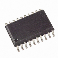
ATTINY261-20SU Atmel, ATTINY261-20SU Datasheet - Page 63

ATTINY261-20SU
Manufacturer Part Number
ATTINY261-20SU
Description
IC MCU AVR 2K FLASH 20MHZ 20SOIC
Manufacturer
Atmel
Series
AVR® ATtinyr
Specifications of ATTINY261-20SU
Core Processor
AVR
Core Size
8-Bit
Speed
20MHz
Connectivity
USI
Peripherals
Brown-out Detect/Reset, POR, PWM, WDT
Number Of I /o
16
Program Memory Size
2KB (1K x 16)
Program Memory Type
FLASH
Eeprom Size
128 x 8
Ram Size
128 x 8
Voltage - Supply (vcc/vdd)
2.7 V ~ 5.5 V
Data Converters
A/D 11x10b
Oscillator Type
Internal
Operating Temperature
-40°C ~ 85°C
Package / Case
20-SOIC (7.5mm Width)
Processor Series
ATTINY2x
Core
AVR8
Data Bus Width
8 bit
Data Ram Size
128 B
Interface Type
SPI, USI
Maximum Clock Frequency
20 MHz
Number Of Programmable I/os
16
Number Of Timers
3
Operating Supply Voltage
2.7 V to 5.5 V
Maximum Operating Temperature
+ 125 C
Mounting Style
SMD/SMT
3rd Party Development Tools
EWAVR, EWAVR-BL
Development Tools By Supplier
ATAVRDRAGON, ATSTK500, ATSTK600, ATAVRISP2, ATAVRONEKIT
Minimum Operating Temperature
- 55 C
On-chip Adc
10 bit, 11 Channel
For Use With
ATSTK600 - DEV KIT FOR AVR/AVR32ATAVRBC100 - REF DESIGN KIT BATTERY CHARGER770-1007 - ISP 4PORT ATMEL AVR MCU SPI/JTAG770-1004 - ISP 4PORT FOR ATMEL AVR MCU SPIATSTK505 - ADAPTER KIT FOR 14PIN AVR MCU
Lead Free Status / RoHS Status
Lead free / RoHS Compliant
Available stocks
Company
Part Number
Manufacturer
Quantity
Price
Part Number:
ATTINY261-20SU
Manufacturer:
ATMEL/爱特梅尔
Quantity:
20 000
- Current page: 63 of 242
- Download datasheet (5Mb)
10.2.1
2588E–AVR–08/10
Alternate Functions of Port A
The Port A pins with alternate function are shown in
Table 10-3.
• Port A, Bit 7 – ADC6/AIN0/PCINT7
• Port A, Bit 6 – ADC5/AIN1/PCINT6
• ADC6: Analog to Digital Converter, Channel 6
• AIN0: Analog Comparator Input. Configure the port pin as input with the internal pull-up
• PCINT7: Pin Change Interrupt source 8.
• ADC5: Analog to Digital Converter, Channel 5.
• AIN1: Analog Comparator Input. Configure the port pin as input with the internal pull-up
• PCINT6: Pin Change Interrupt source 6.
switched off to avoid the digital port function from interfering with the function of the Analog
Comparator.
switched off to avoid the digital port function from interfering with the function of the Analog
Comparator.
Port Pin
PA7
PA6
PA5
PA4
PA3
PA2
PA1
PA0
Port B Pins Alternate Functions
Alternate Function
ADC6:
AIN0:
PCINT7: Pin Change Interrupt 0, Source 7
ADC5:
AIN1:
PCINT6: Pin Change Interrupt 0, Source 6
ADC4:
AIN2:
PCINT5: Pin Change Interrupt 0, Source 5
ADC3:
ICP0:
PCINT4: Pin Change Interrupt 0, Source 4
AREF:
PCINT3: Pin Change Interrupt 0, Source 3
ADC2:
INT1:
USCK: USI Clock (Three Wire Mode)
SCL :
PCINT2: Pin Change Interrupt 0, Source 2
ADC1:
DO:
PCINT1:Pin Change Interrupt 0, Source 1
ADC0:
DI:
SDA:
PCINT0: Pin Change Interrupt 0, Source 0
ADC Input Channel 6
Analog Comparator Input
ADC Input Channel 5
Analog Comparator Input
ADC Input Channel 4
Analog Comparator Input
ADC Input Channel 3
Timer/Counter0 Input Capture Pin
External Analog Reference
ADC Input Channel 2
External Interrupt 1 Input
USI Clock (Two Wire Mode)
ADC Input Channel 1
USI Data Output (Three Wire Mode)
ADC Input Channel 0
USI Data Input (Three Wire Mode)
USI Data Input (Two Wire Mode)
.
Table
10-3.
63
Related parts for ATTINY261-20SU
Image
Part Number
Description
Manufacturer
Datasheet
Request
R

Part Number:
Description:
Manufacturer:
Atmel Corporation
Datasheet:

Part Number:
Description:
Manufacturer:
Atmel Corporation
Datasheet:

Part Number:
Description:
IC MCU AVR 2K FLASH 20MHZ 32-QFN
Manufacturer:
Atmel
Datasheet:

Part Number:
Description:
IC MCU AVR 2K FLASH 20MHZ 20-DIP
Manufacturer:
Atmel
Datasheet:

Part Number:
Description:
MCU AVR 2K FLASH 15MHZ 32-QFN
Manufacturer:
Atmel
Datasheet:

Part Number:
Description:
MCU AVR 2KB FLASH 15MHZ 32-VQFN
Manufacturer:
Atmel
Datasheet:

Part Number:
Description:
Attiny261 8-bit Microcontroller With 2/4/8k Bytes In-system Programmable Flash
Manufacturer:
ATMEL Corporation
Datasheet:

Part Number:
Description:
IC MCU AVR 2K FLASH 20MHZ 20SOIC
Manufacturer:
Atmel
Datasheet:

Part Number:
Description:
IC MCU AVR 2K FLASH 20MHZ 32QFN
Manufacturer:
Atmel
Datasheet:

Part Number:
Description:
Manufacturer:
Atmel Corporation
Datasheet:


