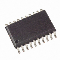
ATTINY261-20SU Atmel, ATTINY261-20SU Datasheet - Page 124

ATTINY261-20SU
Manufacturer Part Number
ATTINY261-20SU
Description
IC MCU AVR 2K FLASH 20MHZ 20SOIC
Manufacturer
Atmel
Series
AVR® ATtinyr
Specifications of ATTINY261-20SU
Core Processor
AVR
Core Size
8-Bit
Speed
20MHz
Connectivity
USI
Peripherals
Brown-out Detect/Reset, POR, PWM, WDT
Number Of I /o
16
Program Memory Size
2KB (1K x 16)
Program Memory Type
FLASH
Eeprom Size
128 x 8
Ram Size
128 x 8
Voltage - Supply (vcc/vdd)
2.7 V ~ 5.5 V
Data Converters
A/D 11x10b
Oscillator Type
Internal
Operating Temperature
-40°C ~ 85°C
Package / Case
20-SOIC (7.5mm Width)
Processor Series
ATTINY2x
Core
AVR8
Data Bus Width
8 bit
Data Ram Size
128 B
Interface Type
SPI, USI
Maximum Clock Frequency
20 MHz
Number Of Programmable I/os
16
Number Of Timers
3
Operating Supply Voltage
2.7 V to 5.5 V
Maximum Operating Temperature
+ 125 C
Mounting Style
SMD/SMT
3rd Party Development Tools
EWAVR, EWAVR-BL
Development Tools By Supplier
ATAVRDRAGON, ATSTK500, ATSTK600, ATAVRISP2, ATAVRONEKIT
Minimum Operating Temperature
- 55 C
On-chip Adc
10 bit, 11 Channel
For Use With
ATSTK600 - DEV KIT FOR AVR/AVR32ATAVRBC100 - REF DESIGN KIT BATTERY CHARGER770-1007 - ISP 4PORT ATMEL AVR MCU SPI/JTAG770-1004 - ISP 4PORT FOR ATMEL AVR MCU SPIATSTK505 - ADAPTER KIT FOR 14PIN AVR MCU
Lead Free Status / RoHS Status
Lead free / RoHS Compliant
Available stocks
Company
Part Number
Manufacturer
Quantity
Price
Part Number:
ATTINY261-20SU
Manufacturer:
ATMEL/爱特梅尔
Quantity:
20 000
- Current page: 124 of 242
- Download datasheet (5Mb)
12.12.15 DT1 – Timer/Counter1 Dead Time Value
124
ATtiny261/461/861
the corresponding interrupt handling vector. Alternatively, OCF1A is cleared, after synchroniza-
tion clock cycle, by writing a logic one to the flag. When the I-bit in SREG, OCIE1A, and OCF1A
are set (one), the Timer/Counter1 A compare match interrupt is executed.
• Bit 5 – OCF1B: Output Compare Flag 1B
The OCF1B bit is set (one) when compare match occurs between Timer/Counter1 and the data
value in OCR1B - Output Compare Register 1A. OCF1B is cleared by hardware when executing
the corresponding interrupt handling vector. Alternatively, OCF1B is cleared, after synchroniza-
tion clock cycle, by writing a logic one to the flag. When the I-bit in SREG, OCIE1B, and OCF1B
are set (one), the Timer/Counter1 B compare match interrupt is executed.
• Bit 2 – TOV1: Timer/Counter1 Overflow Flag
In Normal Mode and Fast PWM Mode the TOV1 bit is set (one) each time the counter reaches
TOP at the same clock cycle when the counter is reset to BOTTOM. In Phase and Frequency
Correct PWM Mode the TOV1 bit is set (one) each time the counter reaches BOTTOM at the
same clock cycle when zero is clocked to the counter.
The bit TOV1 is cleared by hardware when executing the corresponding interrupt handling vec-
tor. Alternatively, TOV1 is cleared, after synchronization clock cycle, by writing a logical one to
the flag. When the SREG I-bit, and TOIE1 (Timer/Counter1 Overflow Interrupt Enable), and
TOV1 are set (one), the Timer/Counter1 Overflow interrupt is executed.
The dead time value register is an 8-bit read/write register.
The dead time delay of all Timer/Counter1 channels are adjusted by the dead time value regis-
ter, DT1. The register consists of two fields, DT1H3:0 and DT1L3:0, one for each
complementary output. Therefore a different dead time delay can be adjusted for the rising edge
of OC1x and the rising edge of OC1x.
• Bits 7:4 – DT1H3:DT1H0: Dead Time Value for OC1x Output
The dead time value for the OC1x output. The dead time delay is set as a number of the pres-
caled timer/counter clocks. The minimum dead time is zero and the maximum dead time is the
prescaled time/counter clock period multiplied by 15.
• Bits 3:0 – DT1L3:DT1L0: Dead Time Value for OC1x Output
The dead time value for the OC1x output. The dead time delay is set as a number of the pres-
caled timer/counter clocks. The minimum dead time is zero and the maximum dead time is the
prescaled time/counter clock period multiplied by 15.
Bit
0x24 (0x44)
Read/Write
Initial value
DT1H3
R/W
7
0
DT1H2
R/W
6
0
DT1H1
R/W
5
0
DT1H0
R/W
4
0
DT1L3
R/W
3
0
DT1L2
R/W
2
0
DT1L1
R/W
1
0
DT1L0
R/W
0
0
2588E–AVR–08/10
DT1
Related parts for ATTINY261-20SU
Image
Part Number
Description
Manufacturer
Datasheet
Request
R

Part Number:
Description:
Manufacturer:
Atmel Corporation
Datasheet:

Part Number:
Description:
Manufacturer:
Atmel Corporation
Datasheet:

Part Number:
Description:
IC MCU AVR 2K FLASH 20MHZ 32-QFN
Manufacturer:
Atmel
Datasheet:

Part Number:
Description:
IC MCU AVR 2K FLASH 20MHZ 20-DIP
Manufacturer:
Atmel
Datasheet:

Part Number:
Description:
MCU AVR 2K FLASH 15MHZ 32-QFN
Manufacturer:
Atmel
Datasheet:

Part Number:
Description:
MCU AVR 2KB FLASH 15MHZ 32-VQFN
Manufacturer:
Atmel
Datasheet:

Part Number:
Description:
Attiny261 8-bit Microcontroller With 2/4/8k Bytes In-system Programmable Flash
Manufacturer:
ATMEL Corporation
Datasheet:

Part Number:
Description:
IC MCU AVR 2K FLASH 20MHZ 20SOIC
Manufacturer:
Atmel
Datasheet:

Part Number:
Description:
IC MCU AVR 2K FLASH 20MHZ 32QFN
Manufacturer:
Atmel
Datasheet:

Part Number:
Description:
Manufacturer:
Atmel Corporation
Datasheet:


