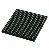
MCIMX512DJM8C Freescale Semiconductor, MCIMX512DJM8C Datasheet - Page 83

MCIMX512DJM8C
Manufacturer Part Number
MCIMX512DJM8C
Description
MULTIMEDIA PROC 529-LFBGA
Manufacturer
Freescale Semiconductor
Series
i.MX51r
Specifications of MCIMX512DJM8C
Core Processor
ARM Cortex-A8
Core Size
32-Bit
Speed
800MHz
Connectivity
1-Wire, EBI/EMI, Ethernet, I²C, IrDA, MMC, SPI, SSI, UART/USART, USB OTG
Peripherals
DMA, I²S, LCD, POR, PWM, WDT
Number Of I /o
128
Program Memory Type
ROMless
Ram Size
128K x 8
Voltage - Supply (vcc/vdd)
0.8 V ~ 1.15 V
Oscillator Type
External
Operating Temperature
-20°C ~ 85°C
Package / Case
529-LFBGA
Processor Series
i.MX51
Core
ARM Cortex A8
Data Bus Width
32 bit
Program Memory Size
36 KB
Data Ram Size
128 KB
Interface Type
I2C, SPI, SSI, UART, USB
Maximum Clock Frequency
200 MHz
Number Of Timers
5
Operating Supply Voltage
0.8 V to 1.15 V
Maximum Operating Temperature
+ 85 C
Mounting Style
SMD/SMT
3rd Party Development Tools
MDK-ARM, RL-ARM, ULINK2
Development Tools By Supplier
MCIMX51EVKJ
Minimum Operating Temperature
- 20 C
Lead Free Status / RoHS Status
Lead free / RoHS Compliant
Eeprom Size
-
Program Memory Size
-
Data Converters
-
Lead Free Status / Rohs Status
Lead free / RoHS Compliant
Available stocks
Company
Part Number
Manufacturer
Quantity
Price
Company:
Part Number:
MCIMX512DJM8C
Manufacturer:
Freescale Semiconductor
Quantity:
10 000
Part Number:
MCIMX512DJM8C
Manufacturer:
FREESCALE
Quantity:
20 000
4.7.8
The purpose of the IPU is to provide comprehensive support for the flow of data from an image sensor
and/or to a display device. This support covers all aspects of these activities:
4.7.8.1
There are three camera timing modes supported by the IPU.
4.7.8.1.1
Smart camera sensors, which include imaging processing, usually support video mode transfer. They use
an embedded timing syntax to replace the SENSB_VSYNC and SENSB_HSYNC signals. The timing
syntax is defined by the BT.656/BT.1120 standards.
This operation mode follows the recommendations of ITU BT.656/ ITU BT.1120 specifications. The only
control signal used is SENSB_PIX_CLK. Start-of-frame and active-line signals are embedded in the data
stream. An active line starts with a SAV code and ends with a EAV code. In some cases, digital blanking
is inserted in between EAV and SAV code. The CSI decodes and filters out the timing-coding from the data
stream, thus recovering SENSB_VSYNC and SENSB_HSYNC signals for internal use. On BT.656 one
component per cycle is received over the SENSB_DATA bus. On BT.1120 two components per cycle are
received over the SENSB_DATA bus.
4.7.8.1.2
The SENSB_VSYNC, SENSB_HSYNC, and SENSB_PIX_CLK signals are used in this mode. See
Figure
Freescale Semiconductor
•
•
•
49.
Connectivity to relevant devices
Related image processing and manipulation: display processing, image conversions, and other
related functions.
Synchronization and control capabilities such as avoidance of tearing artifacts.
SENSB_DATA[19:0] invalid
SENSB_PIX_CLK
SENSB_HSYNC
SENSB_VSYNC
Image Processing Unit (IPU) Module Parameters
Sensor Interface Timings
BT.656 and BT.1120 Video Mode
Gated Clock Mode
Start of Frame
i.MX51 Applications Processors for Consumer and Industrial Products, Rev. 4
nth frame
Figure 49. Gated Clock Mode Timing Diagram
1st byte
—
cameras, displays, graphics accelerators, and TV encoders.
Active Line
n+1th frame
invalid
1st byte
Electrical Characteristics
83


