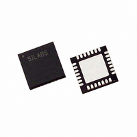
C8051F353-GM Silicon Laboratories Inc, C8051F353-GM Datasheet - Page 52

C8051F353-GM
Manufacturer Part Number
C8051F353-GM
Description
IC 8051 MCU 8K FLASH 28MLP
Manufacturer
Silicon Laboratories Inc
Series
C8051F35xr
Specifications of C8051F353-GM
Program Memory Type
FLASH
Program Memory Size
8KB (8K x 8)
Package / Case
28-VQFN Exposed Pad, 28-HVQFN, 28-SQFN, 28-DHVQFN
Core Processor
8051
Core Size
8-Bit
Speed
50MHz
Connectivity
SMBus (2-Wire/I²C), SPI, UART/USART
Peripherals
POR, PWM, Temp Sensor, WDT
Number Of I /o
17
Ram Size
768 x 8
Voltage - Supply (vcc/vdd)
2.7 V ~ 3.6 V
Data Converters
A/D 8x16b; D/A 2x8b
Oscillator Type
Internal
Operating Temperature
-40°C ~ 85°C
Processor Series
C8051F3x
Core
8051
Data Bus Width
8 bit
Data Ram Size
768 B
Interface Type
I2C/SMBus/SPI/UART
Maximum Clock Frequency
50 MHz
Number Of Programmable I/os
17
Number Of Timers
4
Operating Supply Voltage
2.7 V to 3.6 V
Maximum Operating Temperature
+ 85 C
Mounting Style
SMD/SMT
3rd Party Development Tools
KSK-SL-TOOLSTICK, PK51, CA51, A51, ULINK2
Development Tools By Supplier
C8051F350DK
Minimum Operating Temperature
- 40 C
On-chip Adc
8-ch x 16-bit
On-chip Dac
2-ch x 8-bit
No. Of I/o's
17
Ram Memory Size
768Byte
Cpu Speed
50MHz
No. Of Timers
4
Rohs Compliant
Yes
Package
28QFN
Device Core
8051
Family Name
C8051F35x
Maximum Speed
50 MHz
Data Rom Size
128 B
Height
0.88 mm
Length
5 mm
Supply Voltage (max)
3.6 V
Supply Voltage (min)
2.7 V
Width
5 mm
Lead Free Status / RoHS Status
Lead free / RoHS Compliant
For Use With
770-1006 - ISP 4PORT FOR SILABS C8051F MCU336-1083 - DEV KIT FOR F350/351/352/353
Eeprom Size
-
Lead Free Status / Rohs Status
Lead free / RoHS Compliant
Other names
336-1273
Available stocks
Company
Part Number
Manufacturer
Quantity
Price
Company:
Part Number:
C8051F353-GM
Manufacturer:
SiliconL
Quantity:
8 050
C8051F350/1/2/3
52
Bits 7–0: DECI[7:0]: ADC0 Decimation Ratio Register, Bits 7–0.
This SFR can only be modified when ADC0 is in IDLE mode.
Bits 7–0: ADC0DAC: ADC0 PGA Offset DAC Magnitude.
This SFR can only be modified when ADC0 is in IDLE mode.
DECI7
SFR Definition 5.6. ADC0DECL: ADC0 Decimation Ratio Register Low Byte
R/W
R/W
Bit7
Bit7
This register contains the low byte of the 11-bit ADC Decimation Ratio. The decimation ratio
determines the number of modulator input samples used to generate a single output word
from the ADC.
The ADC0 decimation ratio is defined as:
Decimation Ratio = DECI[10:0] + 1
The corresponding sampling period and output word rate of ADC0 is:
ADC0 Conversion Period = [(DECI[10:0] + 1) * 128] / MDCLK
ADC0 Output Word Rate = MDCLK / [128 * (DECI[10:0] + 1)]
The minimum decimation ratio setting is 20. Any register setting below 19 will automatically
be interpreted as 19.
Important: When using the fast filter, the decimation ratio must be divisible by 8
(DECI[2:0] = 111b).
This register determines the ADC0 Offset DAC Magnitude. The value in the offset DAC is a
signed-magnitude representation. Bit 7 represents the sign value (0 = positive, 1 = nega-
tive), while Bits 6–0 represent the magnitude.
DECI6
R/W
R/W
Bit6
Bit6
SFR Definition 5.7. ADC0DAC: ADC0 Offset DAC
DECI5
R/W
R/W
Bit5
Bit5
DECI4
R/W
R/W
Bit4
Bit4
ADC0DAC
Rev. 1.1
DECI3
R/W
R/W
Bit3
Bit3
DECI2
R/W
R/W
Bit2
Bit2
DECI1
R/W
R/W
Bit1
Bit1
SFR Address:
SFR Address:
DECI0
R/W
R/W
Bit0
Bit0
0x9A
0xBF
00000000
Reset Value
Reset Value
11111111


