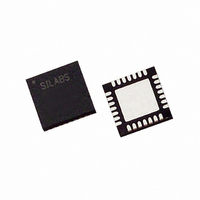
C8051F353-GM Silicon Laboratories Inc, C8051F353-GM Datasheet - Page 221

C8051F353-GM
Manufacturer Part Number
C8051F353-GM
Description
IC 8051 MCU 8K FLASH 28MLP
Manufacturer
Silicon Laboratories Inc
Series
C8051F35xr
Specifications of C8051F353-GM
Program Memory Type
FLASH
Program Memory Size
8KB (8K x 8)
Package / Case
28-VQFN Exposed Pad, 28-HVQFN, 28-SQFN, 28-DHVQFN
Core Processor
8051
Core Size
8-Bit
Speed
50MHz
Connectivity
SMBus (2-Wire/I²C), SPI, UART/USART
Peripherals
POR, PWM, Temp Sensor, WDT
Number Of I /o
17
Ram Size
768 x 8
Voltage - Supply (vcc/vdd)
2.7 V ~ 3.6 V
Data Converters
A/D 8x16b; D/A 2x8b
Oscillator Type
Internal
Operating Temperature
-40°C ~ 85°C
Processor Series
C8051F3x
Core
8051
Data Bus Width
8 bit
Data Ram Size
768 B
Interface Type
I2C/SMBus/SPI/UART
Maximum Clock Frequency
50 MHz
Number Of Programmable I/os
17
Number Of Timers
4
Operating Supply Voltage
2.7 V to 3.6 V
Maximum Operating Temperature
+ 85 C
Mounting Style
SMD/SMT
3rd Party Development Tools
KSK-SL-TOOLSTICK, PK51, CA51, A51, ULINK2
Development Tools By Supplier
C8051F350DK
Minimum Operating Temperature
- 40 C
On-chip Adc
8-ch x 16-bit
On-chip Dac
2-ch x 8-bit
No. Of I/o's
17
Ram Memory Size
768Byte
Cpu Speed
50MHz
No. Of Timers
4
Rohs Compliant
Yes
Package
28QFN
Device Core
8051
Family Name
C8051F35x
Maximum Speed
50 MHz
Data Rom Size
128 B
Height
0.88 mm
Length
5 mm
Supply Voltage (max)
3.6 V
Supply Voltage (min)
2.7 V
Width
5 mm
Lead Free Status / RoHS Status
Lead free / RoHS Compliant
For Use With
770-1006 - ISP 4PORT FOR SILABS C8051F MCU336-1083 - DEV KIT FOR F350/351/352/353
Eeprom Size
-
Lead Free Status / Rohs Status
Lead free / RoHS Compliant
Other names
336-1273
Available stocks
Company
Part Number
Manufacturer
Quantity
Price
Company:
Part Number:
C8051F353-GM
Manufacturer:
SiliconL
Quantity:
8 050
The WDT reset is generated when PCA0L overflows while there is a match between PCA0CPH2 and
PCA0H. Software may force a WDT reset by writing a ‘1’ to the CCF2 flag (PCA0CN.2) while the WDT is
enabled.
23.3.2. Watchdog Timer Usage
To configure the WDT, perform the following tasks:
•
•
•
•
•
•
The PCA clock source and Idle mode select cannot be changed while the WDT is enabled. The watchdog
timer is enabled by setting the WDTE or WDLCK bits in the PCA0MD register. When WDLCK is set, the
WDT cannot be disabled until the next system reset. If WDLCK is not set, the WDT is disabled by clearing
the WDTE bit.
The WDT is enabled following any reset. The PCA0 counter clock defaults to the system clock divided by
12, PCA0L defaults to 0x00, and PCA0CPL2 defaults to 0x00. Using Equation 23.4, this results in a WDT
timeout interval of 256 PCA clock cycles, or 3072 system clock cycles. Table 23.3 lists some example tim-
eout intervals for typical system clocks.
Disable the WDT by writing a ‘0’ to the WDTE bit.
Select the desired PCA clock source (with the CPS2–CPS0 bits).
Load PCA0CPL2 with the desired WDT update offset value.
Configure the PCA Idle mode (set CIDL if the WDT should be suspended while the CPU is in Idle
mode).
Enable the WDT by setting the WDTE bit to ‘1’.
Write a value to PCA0CPH2 to reload the WDT.
Equation 23.4. Watchdog Timer Offset in PCA Clocks
Notes:
System Clock (Hz)
1. Assumes SYSCLK / 12 as the PCA clock source, and a PCA0L
2. SYSCLK reset frequency = Internal oscillator frequency divided by 8.
Table 23.3. Watchdog Timer Timeout Intervals
Offset
24,500,000
24,500,000
24,500,000
18,432,000
18,432,000
18,432,000
11,059,200
11,059,200
11,059,200
3,062,500
3,062,500
3,062,500
value of 0x00 at the update time.
32,000
32,000
32,000
=
2
2
2
(
256 PCA 0 CPL 2
×
PCA0CPL2
Rev. 1.1
255
128
255
128
255
128
255
128
255
128
32
32
32
32
32
)
+
(
256 PCA 0 L
Timeout Interval (ms)
–
C8051F350/1/2/3
24576
12384
129.5
3168
32.1
16.2
42.7
21.5
71.1
35.8
33.1
257
4.1
5.5
9.2
)
1
221


