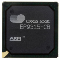
EP9315-CB Cirrus Logic Inc, EP9315-CB Datasheet - Page 56

EP9315-CB
Manufacturer Part Number
EP9315-CB
Description
IC ARM920T MCU 200MHZ 352-PBGA
Manufacturer
Cirrus Logic Inc
Series
EP9r
Specifications of EP9315-CB
Core Processor
ARM9
Core Size
16/32-Bit
Speed
200MHz
Connectivity
EBI/EMI, EIDE, Ethernet, I²C, IrDA, Keypad/Touchscreen, PCMCIA, SPI, UART/USART, USB
Peripherals
AC'97, DMA, I²:S, LCD, LED, MaverickKey, POR, PWM, WDT
Number Of I /o
16
Program Memory Type
ROMless
Ram Size
32K x 8
Voltage - Supply (vcc/vdd)
1.65 V ~ 3.6 V
Data Converters
A/D 8x12b
Oscillator Type
External
Operating Temperature
0°C ~ 70°C
Package / Case
352-BGA
Processor Series
EP93xx
Core
ARM920T
Data Bus Width
32 bit
3rd Party Development Tools
MDK-ARM, RL-ARM, ULINK2
Development Tools By Supplier
EDB9315A-Z
For Use With
598-1144 - KIT DEVELOPMENT EP9315 ARM9
Lead Free Status / RoHS Status
Contains lead / RoHS non-compliant
Eeprom Size
-
Program Memory Size
-
Lead Free Status / Rohs Status
No
Other names
598-1261
Available stocks
Company
Part Number
Manufacturer
Quantity
Price
Part Number:
EP9315-CBZ
Manufacturer:
CIRRUS
Quantity:
20 000
EP9315
Enhanced Universal Platform SOC Processor
352 Pin BGA Pinout (Bottom View)
The following table shows the 352 pin BGA pinout. (For better understanding, compare the coordinates on the x and y
axis on
56
Note:
• VDD_core is CVDD.
• VDD_ring is RVDD.
• All core and ring grounds are connected together and are labelled GND.
• Other special power requirements are clearly labelled (i.e. H18=ADC_VDD and H19=ADC_GND).
• NC means that the pin is not connected.
Figure 40, "352 PIN BGA PINOUT", on page 57
1. Controlling Dimension: Millimeter.
2. Primary Datum C and seating plane are defined by the spherical crowns of the solder balls.
3. Dimension b is measured at the maximum solder ball diameter, parallel to Primary Datum C.
4. There shall be a minimum clearance of 0.25 mm between the edge of the solder ball and the body edge.
5. Reference Document: JEDEC MO-151, BAL-2
Symbol
ddd
D1
D2
D3
A1
A2
E1
E2
E3
A
D
E
b
c
e
q
26.80
23.80
17.95
26.80
23.80
17.95
MIN
©
2.20
1.12
0.51
-
-
-
-
-
-
Copyright 2005 Cirrus Logic (All Rights Reserved)
dimension in mm
Table R. 352 Pin Diagram Dimensions
30° TYP
NOM
27.00
24.13
24.00
18.00
27.00
24.13
24.00
18.00
2.30
0.60
1.17
0.75
0.56
1.27
-
with
MAX
27.20
24.20
18.05
27.20
24.20
18.05
2.50
1.22
0.61
0.15
-
-
-
-
-
Figure 40, "352 Pin PBGA Pin Diagram", on page
1.055
0.087
0.044
0.020
1.055
0.937
0.707
0.937
0.707
MIN
-
-
-
-
-
-
dimension in inches
30° TYP
NOM
0.092
0.024
0.046
0.030
0.022
1.063
0.950
0.945
0.709
1.063
0.950
0.945
0.709
0.050
-
MAX
0.098
0.048
0.024
1.071
0.953
1.071
0.953
0.006
0.711
0.711
-
-
-
-
-
DS638PP4
55.


