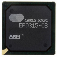
EP9315-CB Cirrus Logic Inc, EP9315-CB Datasheet - Page 36

EP9315-CB
Manufacturer Part Number
EP9315-CB
Description
IC ARM920T MCU 200MHZ 352-PBGA
Manufacturer
Cirrus Logic Inc
Series
EP9r
Specifications of EP9315-CB
Core Processor
ARM9
Core Size
16/32-Bit
Speed
200MHz
Connectivity
EBI/EMI, EIDE, Ethernet, I²C, IrDA, Keypad/Touchscreen, PCMCIA, SPI, UART/USART, USB
Peripherals
AC'97, DMA, I²:S, LCD, LED, MaverickKey, POR, PWM, WDT
Number Of I /o
16
Program Memory Type
ROMless
Ram Size
32K x 8
Voltage - Supply (vcc/vdd)
1.65 V ~ 3.6 V
Data Converters
A/D 8x12b
Oscillator Type
External
Operating Temperature
0°C ~ 70°C
Package / Case
352-BGA
Processor Series
EP93xx
Core
ARM920T
Data Bus Width
32 bit
3rd Party Development Tools
MDK-ARM, RL-ARM, ULINK2
Development Tools By Supplier
EDB9315A-Z
For Use With
598-1144 - KIT DEVELOPMENT EP9315 ARM9
Lead Free Status / RoHS Status
Contains lead / RoHS non-compliant
Eeprom Size
-
Program Memory Size
-
Lead Free Status / Rohs Status
No
Other names
598-1261
Available stocks
Company
Part Number
Manufacturer
Quantity
Price
Part Number:
EP9315-CBZ
Manufacturer:
CIRRUS
Quantity:
20 000
EP9315
Enhanced Universal Platform SOC Processor
Ultra DMA Data Transfer
Figure 21
contains the values for the timings for each of the Ultra DMA modes.
Timing reference levels = 1.5 V
36
Cycle time allowing for asymmetry and clock variations
(from DSTROBE edge to DSTROBE edge)
Two-cycle time allowing for clock variations (from rising edge to next
rising edge or from falling edge to next falling edge of DSTROBE)
Cycle time allowing for asymmetry and clock variations
(from HSTROBE edge to HSTROBE edge)
Two-cycle time allowing for clock variations (from rising edge to next
rising edge or from falling edge to next falling edge of HSTROBE)
Data setup time at recipient (Read)
Data hold time at recipient (Read)
Data valid setup time at sender (Write)
(from data valid until STROBE edge)
Data valid hold time at sender (Write)
(from STROBE edge until data may become invalid)
First STROBE time (for device to first negate DSTROBE from STOP
during a data in burst)
Limited interlock time
Interlock time with minimum
Unlimited interlock time
Maximum time allowed for output drivers to release
(from asserted or negated)
Minimum delay time required for output
Drivers to assert or negate (from released)
Envelope time (from DMACKn to STOP and HDMARDYn during data in
burst initiation and from DMACKn to STOP during data out burst initiation)
Ready-to-final-STROBE time (no STROBE edges shall be sent this long
after negation of DMARDYn)
Ready-to-pause time
(that recipient shall wait to pause after negating DMARDYn)
Maximum time before releasing IORDY
Minimum time before driving STROBE
Setup and hold times for DMACKn (before assertion or negation)
Time from STROBE edge to negation of DMARQ or assertion of STOP
(when sender terminates a burst)
Note:
through
1. Timing parameters shall be measured at the connector of the sender or receiver to which the parameter applies.
2. The test load for t
3. t
4. t
5. All IDE timing is based upon HCLK = 100 MHz.
met for all capacitive loads from 15 to 40 pf where all signals have the same capacitive load value.
other to respond with a signal before proceeding. t
time-out that has a defined minimum. t
UI
ZIORDY
, t
MLI
Figure 30
and t
may be greater than t
Parameter
LI
indicate sender-to-recipient or recipient-to-sender interlocks, i.e., either sender or recipient is waiting for the
DVS
define the timings associated with all phases of Ultra DMA bursts. The following table
and t
©
Copyright 2005 Cirrus Logic (All Rights Reserved)
DVH
ENV
shall be a lumped capacitor load with no cable or receivers. Timing for t
since the device has a pull up on IORDYn giving it a known state when released.
LI
is a limited time-out that has a defined maximum.
(Note 2)
(Note 2)
(Note 3)
(Note 3)
(Note 3)
(Note 4)
UI
is an unlimited interlock that has no maximum time value. t
Symbol
t
t
t
t
t
t
2CYCWR
2CYCRD
CYCWR
IORDYZ
ZIORDY
CYCRD
t
t
t
t
t
t
t
t
t
t
DVS
DVH
t
t
ZAH
ZAD
ENV
RFS
t
ACK
t
MLI
t
DS
DH
t
RP
FS
AZ
SS
UI
LI
min
230
230
460
160
112
15
70
20
20
20
20
50
8
6
0
0
0
0
0
Mode 0
-
-
-
(in ns)
max
230
150
10
70
75
20
-
-
-
-
-
-
-
-
-
-
-
-
-
-
-
-
min
154
170
340
125
73
10
48
20
20
20
20
50
8
6
0
0
0
0
0
Mode 1
-
-
-
(in ns)
max
200
150
10
70
70
20
-
-
-
-
-
-
-
-
-
-
-
-
-
-
-
-
min
115
130
260
100
54
30
20
20
20
20
50
7
8
6
0
0
0
0
0
Mode 2
-
-
-
DVS
(in ns)
and t
max
170
150
10
70
60
20
-
-
-
-
-
-
-
-
-
-
-
-
-
-
-
-
MLI
DVH
is a limited
min
100
200
100
39
86
20
20
20
20
20
50
DS638PP4
shall be
7
8
6
0
0
0
0
0
Mode 3
-
-
-
(in ns)
max
130
100
10
55
60
20
-
-
-
-
-
-
-
-
-
-
-
-
-
-
-
-


