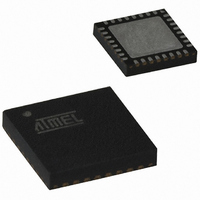
ATTINY261V-10MU Atmel, ATTINY261V-10MU Datasheet - Page 68
ATTINY261V-10MU
Manufacturer Part Number
ATTINY261V-10MU
Description
IC MCU AVR 2K FLASH 10MHZ 32-QFN
Manufacturer
Atmel
Series
AVR® ATtinyr
Datasheet
1.ATAVRMC321.pdf
(242 pages)
Specifications of ATTINY261V-10MU
Core Processor
AVR
Core Size
8-Bit
Speed
10MHz
Connectivity
USI
Peripherals
Brown-out Detect/Reset, POR, PWM, WDT
Number Of I /o
16
Program Memory Size
2KB (1K x 16)
Program Memory Type
FLASH
Eeprom Size
128 x 8
Ram Size
128 x 8
Voltage - Supply (vcc/vdd)
1.8 V ~ 5.5 V
Data Converters
A/D 11x10b
Oscillator Type
Internal
Operating Temperature
-40°C ~ 85°C
Package / Case
32-VQFN Exposed Pad, 32-HVQFN, 32-SQFN, 32-DHVQFN
Processor Series
ATTINY2x
Core
AVR8
Data Bus Width
8 bit
Data Ram Size
128 B
Interface Type
2-Wire, SPI, USI
Maximum Clock Frequency
10 MHz
Number Of Programmable I/os
16
Number Of Timers
2
Maximum Operating Temperature
+ 85 C
Mounting Style
SMD/SMT
Minimum Operating Temperature
- 40 C
On-chip Adc
10 bit, 11 Channel
For Use With
ATSTK600 - DEV KIT FOR AVR/AVR32ATAVRBC100 - REF DESIGN KIT BATTERY CHARGER770-1007 - ISP 4PORT ATMEL AVR MCU SPI/JTAGATSTK505 - ADAPTER KIT FOR 14PIN AVR MCU
Lead Free Status / RoHS Status
Lead free / RoHS Compliant
Available stocks
Company
Part Number
Manufacturer
Quantity
Price
Company:

Part Number:
ATTINY261V-10MU
Manufacturer:
Atmel
Quantity:
1 962


68
ATtiny261/461/861
• Port B, Bit 1 – MISO/ DO/ OC1A/ PCINT9
• Port B, Bit 0 – MOSI/ DI/ SDA/ OC1A/ PCINT8
Table 10-7
shown in
Table 10-7.
Note:
Signal
Name
PUOE
PUOV
DDOE
DDOV
PVOE
PVOV
PTOE
DIEOE
DIEOV
DI
AIO
• DO: Three-wire mode Universal Serial Interface Data output. Three-wire mode Data output
• OC1A: Output Compare Match output: The PB1 pin can serve as an external output for the
• PCINT9: Pin Change Interrupt source 9.
• DI: Data Input in USI Three-wire mode. USI Three-wire mode does not override normal port
• SDA: Two-wire mode Serial Interface Data.
• OC1A: Inverted Output Compare Match output: The PB0 pin can serve as an external output
• PCINT8: Pin Change Interrupt source 8.
overrides PORTB1 value and it is driven to the port when data direction bit DDB1 is set (one).
PORTB1 still enables the pull-up, if the direction is input and PORTB1 is set (one).
Timer/Counter1 Compare Match B when configured as an output (DDB1 set). The OC1A pin
is also the output pin for the PWM mode timer function.
functions, so pin must be configure as an input for DI function.
for the Timer/Counter1 Compare Match B when configured as an output (DDB0 set). The
OC1A pin is also the inverted output pin for the PWM mode timer function.
1. “1” when the Fuse is “0” (Programmed).
Figure 10-5 on page
PB7/RESET/
dW/ADC10/
PCINT15
RSTDISBL
DWEN
1
RSTDISBL
DWEN
debugWire Transmit
0
0
0
0
ADC10D
PCINT15
RESET / ADC10
and
Overriding Signals for Alternate Functions in PB7:PB4
Table 10-8
(1)
(1)
(1)
(1)
•
•
relate the alternate functions of Port B to the overriding signals
61.
PB6/ADC9/T0/
INT0/PCINT14
0
0
0
0
0
0
0
RSTDISBL + (PCINT5
• PCIE + ADC9D)
ADC9D
T0/INT0/PCINT14
ADC9
PB5/XTAL2/CLKO/
OC1D/ADC8/
PCINT13
INTRC • EXTCLK
0
INTRC • EXTCLK
0
OC1D Enable
OC1D
0
INTRC • EXTCLK +
PCINT4 • PCIE +
ADC8D
(INTRC • EXTCLK) +
ADC8D
PCINT13
XTAL2, ADC8
(1)
PB4/XTAL1/
OC1D/ADC7/
PCINT12
INTRC
0
INTRC
0
OC1D Enable
OC1D
0
INTRC + PCINT12 •
PCIE + ADC7D
INTRC • ADC7D
PCINT12
XTAL1, ADC7
2588E–AVR–08/10
(1)
Related parts for ATTINY261V-10MU
Image
Part Number
Description
Manufacturer
Datasheet
Request
R

Part Number:
Description:
Manufacturer:
Atmel Corporation
Datasheet:
Part Number:
Description:
Manufacturer:
Atmel Corporation
Datasheet:

Part Number:
Description:
IC MCU AVR 2K FLASH 20MHZ 32-QFN
Manufacturer:
Atmel
Datasheet:

Part Number:
Description:
IC MCU AVR 2K FLASH 20MHZ 20-DIP
Manufacturer:
Atmel
Datasheet:

Part Number:
Description:
MCU AVR 2K FLASH 15MHZ 32-QFN
Manufacturer:
Atmel
Datasheet:
Part Number:
Description:
MCU AVR 2KB FLASH 15MHZ 32-VQFN
Manufacturer:
Atmel
Datasheet:

Part Number:
Description:
IC MCU AVR 2K FLASH 20MHZ 20SOIC
Manufacturer:
Atmel
Datasheet:
Part Number:
Description:
Attiny261 8-bit Microcontroller With 2/4/8k Bytes In-system Programmable Flash
Manufacturer:
ATMEL Corporation
Datasheet:

Part Number:
Description:
IC MCU AVR 2K FLASH 20MHZ 20SOIC
Manufacturer:
Atmel
Datasheet:
Part Number:
Description:
IC MCU AVR 2K FLASH 20MHZ 32QFN
Manufacturer:
Atmel
Datasheet: