ATTINY261V-10MU Atmel, ATTINY261V-10MU Datasheet - Page 3
ATTINY261V-10MU
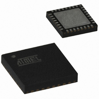
Manufacturer Part Number
ATTINY261V-10MU
Description
IC MCU AVR 2K FLASH 10MHZ 32-QFN
Manufacturer
Atmel
Series
AVR® ATtinyr
Datasheet
1.ATAVRMC321.pdf
(242 pages)
Specifications of ATTINY261V-10MU
Core Processor
AVR
Core Size
8-Bit
Speed
10MHz
Connectivity
USI
Peripherals
Brown-out Detect/Reset, POR, PWM, WDT
Number Of I /o
16
Program Memory Size
2KB (1K x 16)
Program Memory Type
FLASH
Eeprom Size
128 x 8
Ram Size
128 x 8
Voltage - Supply (vcc/vdd)
1.8 V ~ 5.5 V
Data Converters
A/D 11x10b
Oscillator Type
Internal
Operating Temperature
-40°C ~ 85°C
Package / Case
32-VQFN Exposed Pad, 32-HVQFN, 32-SQFN, 32-DHVQFN
Processor Series
ATTINY2x
Core
AVR8
Data Bus Width
8 bit
Data Ram Size
128 B
Interface Type
2-Wire, SPI, USI
Maximum Clock Frequency
10 MHz
Number Of Programmable I/os
16
Number Of Timers
2
Maximum Operating Temperature
+ 85 C
Mounting Style
SMD/SMT
Minimum Operating Temperature
- 40 C
On-chip Adc
10 bit, 11 Channel
For Use With
ATSTK600 - DEV KIT FOR AVR/AVR32ATAVRBC100 - REF DESIGN KIT BATTERY CHARGER770-1007 - ISP 4PORT ATMEL AVR MCU SPI/JTAGATSTK505 - ADAPTER KIT FOR 14PIN AVR MCU
Lead Free Status / RoHS Status
Lead free / RoHS Compliant
Available stocks
Company
Part Number
Manufacturer
Quantity
Price
Company:

Part Number:
ATTINY261V-10MU
Manufacturer:
Atmel
Quantity:
1 962


1.1
1.1.1
1.1.2
1.1.3
1.1.4
1.1.5
1.1.6
1.1.7
2588E–AVR–08/10
Pin Descriptions
VCC
GND
AVCC
AGND
Port A (PA7:PA0)
Port B (PB7:PB0)
RESET
Supply voltage.
Ground.
Analog supply voltage. This is the supply voltage pin for the Analog-to-digital Converter (ADC),
the analog comparator, the Brown-Out Detector (BOD), the internal voltage reference and Port
A. It should be externally connected to VCC, even if some peripherals such as the ADC are not
used. If the ADC is used AVCC should be connected to VCC through a low-pass filter.
Analog ground.
An 8-bit, bi-directional I/O port with internal pull-up resistors, individually selectable for each bit.
Output buffers have symmetrical drive characteristics with both high sink and source capability.
As inputs, port pins that are externally pulled low will source current if pull-up resistors have
been activated. Port pins are tri-stated when a reset condition becomes active, even if the clock
is not running.
Port A also serves the functions of various special features of the device, as listed on
An 8-bit, bi-directional I/O port with internal pull-up resistors, individually selectable for each bit.
Output buffers have symmetrical drive characteristics with both high sink and source capability.
As inputs, port pins that are externally pulled low will source current if pull-up resistors have
been activated. Port pins are tri-stated when a reset condition becomes active, even if the clock
is not running.
Port B also serves the functions of various special features of the device, as listed on
Reset input. A low level on this pin for longer than the minimum pulse length will generate a
reset, even if the clock is not running and provided the reset pin has not been disabled. The min-
imum pulse length is given in
generate a reset.
The reset pin can also be used as a (weak) I/O pin.
Table 19-4 on page
190. Shorter pulses are not guaranteed to
page
page
63.
66.
3
Related parts for ATTINY261V-10MU
Image
Part Number
Description
Manufacturer
Datasheet
Request
R

Part Number:
Description:
Manufacturer:
Atmel Corporation
Datasheet:
Part Number:
Description:
Manufacturer:
Atmel Corporation
Datasheet:

Part Number:
Description:
IC MCU AVR 2K FLASH 20MHZ 32-QFN
Manufacturer:
Atmel
Datasheet:

Part Number:
Description:
IC MCU AVR 2K FLASH 20MHZ 20-DIP
Manufacturer:
Atmel
Datasheet:

Part Number:
Description:
MCU AVR 2K FLASH 15MHZ 32-QFN
Manufacturer:
Atmel
Datasheet:
Part Number:
Description:
MCU AVR 2KB FLASH 15MHZ 32-VQFN
Manufacturer:
Atmel
Datasheet:

Part Number:
Description:
IC MCU AVR 2K FLASH 20MHZ 20SOIC
Manufacturer:
Atmel
Datasheet:
Part Number:
Description:
Attiny261 8-bit Microcontroller With 2/4/8k Bytes In-system Programmable Flash
Manufacturer:
ATMEL Corporation
Datasheet:

Part Number:
Description:
IC MCU AVR 2K FLASH 20MHZ 20SOIC
Manufacturer:
Atmel
Datasheet:
Part Number:
Description:
IC MCU AVR 2K FLASH 20MHZ 32QFN
Manufacturer:
Atmel
Datasheet: