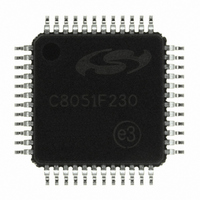
C8051F230-GQ Silicon Laboratories Inc, C8051F230-GQ Datasheet - Page 92

C8051F230-GQ
Manufacturer Part Number
C8051F230-GQ
Description
IC 8051 MCU 8K FLASH 48TQFP
Manufacturer
Silicon Laboratories Inc
Series
C8051F2xxr
Specifications of C8051F230-GQ
Program Memory Type
FLASH
Program Memory Size
8KB (8K x 8)
Package / Case
48-TQFP, 48-VQFP
Core Processor
8051
Core Size
8-Bit
Speed
25MHz
Connectivity
SPI, UART/USART
Peripherals
Brown-out Detect/Reset, POR, WDT
Number Of I /o
32
Ram Size
256 x 8
Voltage - Supply (vcc/vdd)
2.7 V ~ 3.6 V
Oscillator Type
Internal
Operating Temperature
-40°C ~ 85°C
Processor Series
C8051F2x
Core
8051
Data Bus Width
8 bit
Data Ram Size
256 B
Interface Type
SPI/UART
Maximum Clock Frequency
25 MHz
Number Of Programmable I/os
32
Number Of Timers
3
Operating Supply Voltage
2.7 V to 3.6 V
Maximum Operating Temperature
+ 85 C
Mounting Style
SMD/SMT
3rd Party Development Tools
PK51, CA51, A51, ULINK2
Development Tools By Supplier
C8051F226DK
Minimum Operating Temperature
- 40 C
No. Of I/o's
32
Ram Memory Size
256Byte
Cpu Speed
25MHz
No. Of Timers
3
Rohs Compliant
Yes
Package
48TQFP
Device Core
8051
Family Name
C8051F2xx
Maximum Speed
25 MHz
Lead Free Status / RoHS Status
Lead free / RoHS Compliant
Eeprom Size
-
Data Converters
-
Lead Free Status / Rohs Status
Lead free / RoHS Compliant
Other names
336-1242
Available stocks
Company
Part Number
Manufacturer
Quantity
Price
Company:
Part Number:
C8051F230-GQ
Manufacturer:
SiliconL
Quantity:
138
Company:
Part Number:
C8051F230-GQ
Manufacturer:
Silicon Laboratories Inc
Quantity:
10 000
Company:
Part Number:
C8051F230-GQR
Manufacturer:
Silicon Laboratories Inc
Quantity:
10 000
C8051F2xx
12.1. Power-on Reset
The CIP-51 incorporates a power supply monitor that holds the MCU in the reset state until V
above the VRST level during power-up. (See Figure 12.2 for timing diagram, and refer to Table 12.1 for
the Electrical Characteristics of the power supply monitor circuit.) The RST pin is asserted (low) until the
end of the 100msec V
packages, the V
MONEN pin low. The MONEN pin should never be left floating. On 32-pin packages, the V
always enabled and cannot be disabled.
On exit from a power-on reset, the PORSF flag (RSTSRC.1) is set by hardware to logic 1. All of the other
reset flags in the RSTSRC Register are indeterminate. PORSF is cleared by all other resets. Since all
resets cause program execution to begin at the same location (0x0000), software can read the PORSF
flag to determine if a power-up was the cause of reset. The content of internal data memory should be
assumed to be undefined after a power-on reset.
12.2. Software Forced Reset
Writing a 1 to the PORSF bit forces a Power-On Reset as described in Section 12.1.
12.3. Power-fail Reset
When the V
and power-down transition or power irregularity causes V
will drive the RST pin low and return the CIP-51 to the reset state (see Figure 12.2). When V
a level above VRST, the CIP-51 will leave the reset state in the same manner as that for the power-on
reset. Note that even though internal data memory contents are not altered by the power-fail reset, it is
impossible to determine if V
set, the data may no longer be valid.
92
Logic HIGH
Logic LOW
DD
2.70
2.55
2.0
1.0
monitor is enabled, the MONEN pin (not on C8051F221/F231 32 pin parts) is "pulled high",
DD
monitor is enabled by pulling the MONEN pin high and is disabled by pulling the
/RST
DD
Monitor timeout in order to allow the V
Figure 12.2. V
DD
V
RST
dropped below the level required for data retention. If the PORSF flag is
DD
100ms
Monitor Timing Diagram
Rev. 1.6
DD
to drop below VRST, the power supply monitor
DD
supply to become stable. On 48-pin
100ms
DD
DD
monitor is
returns to
DD
t
rises


