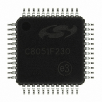
C8051F230-GQ Silicon Laboratories Inc, C8051F230-GQ Datasheet - Page 142

C8051F230-GQ
Manufacturer Part Number
C8051F230-GQ
Description
IC 8051 MCU 8K FLASH 48TQFP
Manufacturer
Silicon Laboratories Inc
Series
C8051F2xxr
Specifications of C8051F230-GQ
Program Memory Type
FLASH
Program Memory Size
8KB (8K x 8)
Package / Case
48-TQFP, 48-VQFP
Core Processor
8051
Core Size
8-Bit
Speed
25MHz
Connectivity
SPI, UART/USART
Peripherals
Brown-out Detect/Reset, POR, WDT
Number Of I /o
32
Ram Size
256 x 8
Voltage - Supply (vcc/vdd)
2.7 V ~ 3.6 V
Oscillator Type
Internal
Operating Temperature
-40°C ~ 85°C
Processor Series
C8051F2x
Core
8051
Data Bus Width
8 bit
Data Ram Size
256 B
Interface Type
SPI/UART
Maximum Clock Frequency
25 MHz
Number Of Programmable I/os
32
Number Of Timers
3
Operating Supply Voltage
2.7 V to 3.6 V
Maximum Operating Temperature
+ 85 C
Mounting Style
SMD/SMT
3rd Party Development Tools
PK51, CA51, A51, ULINK2
Development Tools By Supplier
C8051F226DK
Minimum Operating Temperature
- 40 C
No. Of I/o's
32
Ram Memory Size
256Byte
Cpu Speed
25MHz
No. Of Timers
3
Rohs Compliant
Yes
Package
48TQFP
Device Core
8051
Family Name
C8051F2xx
Maximum Speed
25 MHz
Lead Free Status / RoHS Status
Lead free / RoHS Compliant
Eeprom Size
-
Data Converters
-
Lead Free Status / Rohs Status
Lead free / RoHS Compliant
Other names
336-1242
Available stocks
Company
Part Number
Manufacturer
Quantity
Price
Company:
Part Number:
C8051F230-GQ
Manufacturer:
SiliconL
Quantity:
138
Company:
Part Number:
C8051F230-GQ
Manufacturer:
Silicon Laboratories Inc
Quantity:
10 000
Company:
Part Number:
C8051F230-GQR
Manufacturer:
Silicon Laboratories Inc
Quantity:
10 000
C8051F2xx
142
DATA7 DATA6
This register is used to read or write data to the Flash memory across the JTAG interface.
Bits9–2: DATA7–0: Flash Data Byte.
Bit1:
Bit0:
This register controls the Flash read timing circuit and the prescaler required to generate the correct
timing for Flash operations.
Bit7:
Bit6:
Bits5–4: UNUSED. Read = 00b, Write = don't care.
Bits3–0: FLSCL3–0: Flash Prescaler Control Bits.
FOSE
Bit9
Bit7
FAIL: Flash Fail Bit.
0:
1:
BUSY: Flash Busy Bit.
0:
1:
FOSE: Flash One-Shot Enable Bit.
0: Flash read strobe is a full clock-cycle wide.
1: Flash read strobe is 50nsec.
FRAE: Flash Read Always Bit.
0: The Flash output enable and sense amplifier enable are on only when needed to read the
1: The Flash output enable and sense amplifier enable are always on. This can be used to
The FLSCL3–0 bits control the prescaler used to generate timing signals for Flash opera-
tions. Its value should be written before any Flash write or erase operations are initiated.
The value written should be the smallest integer for which:
FLSCL[3:0] > log2(fSYSCLK / 50kHz)
Where fSYSCLK is the system clock frequency. All Flash read/write/erase operations are
disallowed when FLSCL[3:0] = 1111b.
Bit8
JTAG Register Definition 18.5. FLASHSCL: JTAG Flash Scale
JTAG Register Definition 18.4. FLASHDAT: JTAG Flash Data
FRAE
Flash memory.
limit the variations in digital supply current due to switching the sense amplifiers, thereby
reducing digitally induced noise.
Bit6
DATA5
Previous Flash memory operation was successful.
Previous Flash memory operation failed. Usually indicates the associated memory
location was locked.
Flash interface logic is not busy.
not initiate another operation
Flash interface logic is processing a request. Reads or writes while BUSY = 1 will
Bit7
Bit5
-
DATA4 DATA3 DATA2 DATA1
Bit6
Bit4
-
Bit5
FLSCL3
Rev. 1.6
Bit4
Bit3
Bit3
FLSCL2
Bit2
DATA0
Bit2
FLSCL1
Bit1
FAIL
Bit1
FLSCL0
BUSY
Bit0
Bit0
0000000000
Reset Value
Reset Value
00000000


