ST10F269Z2Q3 STMicroelectronics, ST10F269Z2Q3 Datasheet - Page 93

ST10F269Z2Q3
Manufacturer Part Number
ST10F269Z2Q3
Description
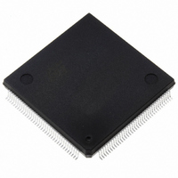
IC FLASH MEM 256KBIT 144-PQFP
Manufacturer
STMicroelectronics
Series
ST10r
Datasheet
1.ST10F269Z2Q3.pdf
(184 pages)
Specifications of ST10F269Z2Q3
Core Processor
ST10
Core Size
16-Bit
Speed
40MHz
Connectivity
CAN, EBI/EMI, SSC, UART/USART
Peripherals
POR, PWM, WDT
Number Of I /o
111
Program Memory Size
256KB (256K x 8)
Program Memory Type
FLASH
Ram Size
12K x 8
Voltage - Supply (vcc/vdd)
4.5 V ~ 5.5 V
Data Converters
A/D 16x10b
Oscillator Type
Internal
Operating Temperature
-40°C ~ 125°C
Package / Case
144-QFP
Processor Series
ST10F26x
Core
ST10
Data Bus Width
16 bit
Data Ram Size
12 KB
Interface Type
CAN, SSC, USART
Maximum Clock Frequency
40 MHz
Number Of Programmable I/os
111
Number Of Timers
2 x 16 bit
Operating Supply Voltage
0.3 V to 4 V
Maximum Operating Temperature
+ 125 C
Mounting Style
SMD/SMT
Minimum Operating Temperature
- 40 C
On-chip Adc
16 bit x 10 bit
Cpu Family
ST10
Device Core Size
16b
Frequency (max)
40MHz
Total Internal Ram Size
12KB
# I/os (max)
111
Number Of Timers - General Purpose
5
Operating Supply Voltage (typ)
5V
Operating Supply Voltage (max)
5.5V
Operating Supply Voltage (min)
4.5V
Instruction Set Architecture
CISC/RISC
Operating Temp Range
-40C to 125C
Operating Temperature Classification
Automotive
Mounting
Surface Mount
Pin Count
144
Package Type
PQFP
Lead Free Status / RoHS Status
Lead free / RoHS Compliant
Eeprom Size
-
Lead Free Status / Rohs Status
Lead free / RoHS Compliant
Other names
497-2042
Available stocks
Company
Part Number
Manufacturer
Quantity
Price
Company:
Part Number:
ST10F269Z2Q3
Manufacturer:
INFINEON
Quantity:
1 443
Company:
Part Number:
ST10F269Z2Q3
Manufacturer:
STMicroelectronics
Quantity:
10 000
Part Number:
ST10F269Z2Q3
Manufacturer:
ST
Quantity:
20 000
ST10F269
13 - A/D CONVERTER
A 10-bit A/D converter with 16 multiplexed input
channels and a sample and hold circuit is
integrated on-chip. The sample time (for loading
the capacitors) and the conversion time is
programmable and can be adjusted to the
external circuitry.
To remove high frequency components from the
analog input signal, a low-pass filter must be con-
nected at the ADC input.
Overrun error detection / protection is controlled
by the ADDAT register. Either an interrupt request
is generated when the result of a previous
conversion has not been read from the result
register at the time the next conversion is
complete, or the next conversion is suspended
until the previous result has been read. For
applications which require less than 16 analog
input channels, the remaining channel inputs can
be used as digital input port pins. The A/D
converter of the ST10F269 supports different
conversion modes:
– Single channel single conversion: the analog
– Single channel continuous conversion: the
– Auto scan single conversion: the analog level
Table 26 : ADC Sample Clock and Conversion Clock (PQFP144 devices)
Notes: 1. Section 21.4.5 -: Direct Drive for TCL definition.
level of the selected channel is sampled once
and converted. The result of the conversion is
stored in the ADDAT register.
analog level of the selected channel is repeated-
ly sampled and converted. The result of the con-
version is stored in the ADDAT register.
of the selected channels are sampled once and
ADCTC
2. t
00
01
10
11
CC
= TCL x 24
Reserved, do not use
TCL
1
TCL x 24
TCL x 96
TCL x 48
= 1/2 x f
Conversion Clock t
XTAL
At f
CPU
Reserved
CC
1.2 s
0.6 s
0.3 s
= 40MHz
– Auto scan continuous conversion: the analog
– Wait for ADDAT read mode: when using con-
– Channel
converted. After each conversion the result is
stored in the ADDAT register. The data can be
transferred to the RAM by interrupt software
management or using the powerful Peripheral
Event Controller (PEC) data transfer.
level of the selected channels are repeatedly
sampled and converted. The result of the con-
version is stored in the ADDAT register. The
data can be transferred to the RAM by interrupt
software management or using the PEC data
transfer.
tinuous modes, in order to avoid to overwrite
the result of the current conversion by the next
one, the ADWR bit of ADCON control register
must be activated. Then, until the ADDAT regis-
ter is read, the new result is stored in a tempo-
rary buffer and the conversion is on hold.
continuous modes, a selected channel can be
converted in between without changing the
current operating mode. The 10-bit data of the
conversion are stored in ADRES field of
ADDAT2. The current continuous mode remains
active after the single conversion is completed
ADSTC
00
01
10
11
injection
t
t
t
CC
CC
CC
t
SC
t
CC
13 - A/D CONVERTER
x 2
x 4
x 8
Sample Clock t
=
mode:
At f
when
CPU
0.3 s
0.6 s
1.2 s
2.4 s
SC
= 40MHz
2
2
2
2
93/184
using


