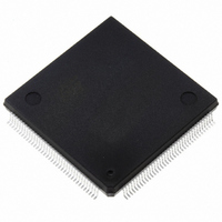
ST10F269Z2Q3 STMicroelectronics, ST10F269Z2Q3 Datasheet - Page 170

ST10F269Z2Q3
Manufacturer Part Number
ST10F269Z2Q3
Description
IC FLASH MEM 256KBIT 144-PQFP
Manufacturer
STMicroelectronics
Series
ST10r
Datasheet
1.ST10F269Z2Q3.pdf
(184 pages)
Specifications of ST10F269Z2Q3
Core Processor
ST10
Core Size
16-Bit
Speed
40MHz
Connectivity
CAN, EBI/EMI, SSC, UART/USART
Peripherals
POR, PWM, WDT
Number Of I /o
111
Program Memory Size
256KB (256K x 8)
Program Memory Type
FLASH
Ram Size
12K x 8
Voltage - Supply (vcc/vdd)
4.5 V ~ 5.5 V
Data Converters
A/D 16x10b
Oscillator Type
Internal
Operating Temperature
-40°C ~ 125°C
Package / Case
144-QFP
Processor Series
ST10F26x
Core
ST10
Data Bus Width
16 bit
Data Ram Size
12 KB
Interface Type
CAN, SSC, USART
Maximum Clock Frequency
40 MHz
Number Of Programmable I/os
111
Number Of Timers
2 x 16 bit
Operating Supply Voltage
0.3 V to 4 V
Maximum Operating Temperature
+ 125 C
Mounting Style
SMD/SMT
Minimum Operating Temperature
- 40 C
On-chip Adc
16 bit x 10 bit
Cpu Family
ST10
Device Core Size
16b
Frequency (max)
40MHz
Total Internal Ram Size
12KB
# I/os (max)
111
Number Of Timers - General Purpose
5
Operating Supply Voltage (typ)
5V
Operating Supply Voltage (max)
5.5V
Operating Supply Voltage (min)
4.5V
Instruction Set Architecture
CISC/RISC
Operating Temp Range
-40C to 125C
Operating Temperature Classification
Automotive
Mounting
Surface Mount
Pin Count
144
Package Type
PQFP
Lead Free Status / RoHS Status
Lead free / RoHS Compliant
Eeprom Size
-
Lead Free Status / Rohs Status
Lead free / RoHS Compliant
Other names
497-2042
Available stocks
Company
Part Number
Manufacturer
Quantity
Price
Company:
Part Number:
ST10F269Z2Q3
Manufacturer:
INFINEON
Quantity:
1 443
Company:
Part Number:
ST10F269Z2Q3
Manufacturer:
STMicroelectronics
Quantity:
10 000
Part Number:
ST10F269Z2Q3
Manufacturer:
ST
Quantity:
20 000
Figure 79 : CLKOUT and READY
Notes: 1. Cycle as programmed, including MCTC wait states (Example shows 0 MCTC WS).
170/184
CLKOUT
ALE
RD, WR
Synchronous
READY
Asynchronous
READY
2. The leading edge of the respective command depends on RW-delay.
3. READY sampled HIGH at this sampling point generates a READY controlled wait state, READY sampled LOW at this sampling
point terminates the currently running bus cycle.
4. READY may be deactivated in response to the trailing (rising) edge of the corresponding command (RD or WR).
5. If the Asynchronous READY signal does not fulfill the indicated setup and hold times with respect to CLKOUT (e.g. because
CLKOUT is not enabled), it must fulfill t
the command (see Note 4)).
6. Multiplexed bus modes have a MUX wait state added after a bus cycle, and an additional MTTC wait state may be inserted here.
For a multiplexed bus with MTTC wait state this delay is 2 CLKOUT cycles, for a demultiplexed bus without MTTC wait state this delay
is zero.
7. The next external bus cycle may start here.
t
t
58
32
3)
t
t
t
59
30
34
Running cycle 1)
37
in order to be safely synchronized. This is guaranteed, if READY is removed in response to
2)
t
t
33
31
t
t
35
58
3)
t
37
3)
t
t
36
59
t
5)
29
t
35
wait state
READY
3)
t
36
MUX / Tri-state 6)
t
60 4)
6)
ST10F269
7)


