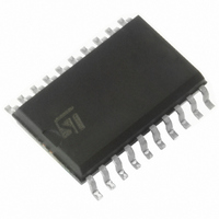
ST7FLITE29F2M6 STMicroelectronics, ST7FLITE29F2M6 Datasheet - Page 62

ST7FLITE29F2M6
Manufacturer Part Number
ST7FLITE29F2M6
Description
IC MCU 8BIT 8K FLASH 20SOIC
Manufacturer
STMicroelectronics
Series
ST7r
Datasheet
1.ST7FLITE20F2B6.pdf
(133 pages)
Specifications of ST7FLITE29F2M6
Core Processor
ST7
Core Size
8-Bit
Speed
8MHz
Connectivity
SPI
Peripherals
LVD, POR, PWM, WDT
Number Of I /o
15
Program Memory Size
8KB (8K x 8)
Program Memory Type
FLASH
Eeprom Size
256 x 8
Ram Size
384 x 8
Voltage - Supply (vcc/vdd)
2.4 V ~ 5.5 V
Data Converters
A/D 7x10b
Oscillator Type
Internal
Operating Temperature
-40°C ~ 85°C
Package / Case
20-SOIC (7.5mm Width)
Processor Series
ST7FLITE2x
Core
ST7
Data Bus Width
8 bit
Data Ram Size
384 B
Interface Type
SPI
Maximum Clock Frequency
8 MHz
Number Of Programmable I/os
15
Number Of Timers
4 bit
Operating Supply Voltage
2.4 V to 5.5 V
Maximum Operating Temperature
+ 85 C
Mounting Style
SMD/SMT
Development Tools By Supplier
ST7FLIT2-COS/COM, ST7FLITE-SK/RAIS, ST7MDT10-DVP3, ST7MDT10-EMU3, STX-RLINK
Minimum Operating Temperature
- 40 C
On-chip Adc
13 bit
For Use With
497-5858 - EVAL BOARD PLAYBACK ST7FLITE497-5049 - KIT STARTER RAISONANCE ST7FLITE497-5046 - KIT TOOL FOR ST7/UPSD/STR7 MCU
Lead Free Status / RoHS Status
Lead free / RoHS Compliant
Other names
497-2135-5
Available stocks
Company
Part Number
Manufacturer
Quantity
Price
Company:
Part Number:
ST7FLITE29F2M6TR
Manufacturer:
ST
Quantity:
5 700
Part Number:
ST7FLITE29F2M6TR
Manufacturer:
ST
Quantity:
20 000
ST7LITE2
12-BIT AUTORELOAD TIMER (Cont’d)
Bit 4 = BPEN Break Pin Enable.
This bit is read/write by software and cleared by
hardware after Reset.
0: Break pin disabled
1: Break pin enabled
Bits 3:0 = PWM[3:0] Break Pattern.
These bits are read/write by software and cleared
by hardware after a reset. They are used to force
the four PWMx output signals into a stable state
when the Break function is active.
PWMx DUTY CYCLE REGISTER HIGH (DCRxH)
Read / Write
Reset Value: 0000 0000 (00h)
PWMx DUTY CYCLE REGISTER LOW (DCRxL)
Read / Write
Reset Value: 0000 0000 (00h)
Bits 15:12 = Reserved.
Bits 11:0 = DCR[11:0] PWMx Duty Cycle Value
This 12-bit value is written by software. It defin-
esthe duty cycle of the corresponding PWM output
signal (see
In PWM mode (OEx=1 in the PWMCR register)
the DCR[11:0] bits define the duty cycle of the
PWMx output signal (see
Compare mode, they define the value to be com-
pared with the 12-bit upcounter value.
62/133
1
DCR7 DCR6 DCR5 DCR4 DCR3 DCR2 DCR1 DCR0
15
0
7
0
Figure
0
36).
0
DCR11 DCR10 DCR9 DCR8
Figure
36). In Output
8
0
INPUT CAPTURE REGISTER HIGH (ATICRH)
Read only
Reset Value: 0000 0000 (00h)
INPUT CAPTURE REGISTER LOW (ATICRL)
Read only
Reset Value: 0000 0000 (00h)
Bits 15:12 = Reserved.
Bits 11:0 = ICR[11:0] Input Capture Data.
This is a 12-bit register which is readable by soft-
ware and cleared by hardware after a reset. The
ATICR register contains captured the value of the
12-bit CNTR register when a rising or falling edge
occurs on the ATIC pin. Capture will only be per-
formed when the ICF flag is cleared.
TRANSFER CONTROL REGISTER (TRANCR)
Read/Write
Reset Value: 0000 0001 (01h)
Bits 7:1 Reserved. Forced by hardware to 0.
Bit 0 = TRAN Transfer enable
This bit is read/write by software, cleared by hard-
ware after each completed transfer and set by
hardware after reset.
It allows the value of the DCRx registers to be
transferred to the DCRx shadow registers after the
next overflow event.
The OPx bits are transferred to the shadow OPx
bits in the same way.
ICR7
15
0
7
7
0
ICR6
0
0
ICR5
0
0
ICR4
0
0
ICR11 ICR10
ICR3
0
ICR2
0
ICR9
ICR1
0
TRAN
ICR8
ICR0
8
0
0


