ATMEGA168-20PU Atmel, ATMEGA168-20PU Datasheet - Page 197
ATMEGA168-20PU
Manufacturer Part Number
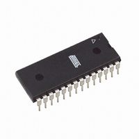
ATMEGA168-20PU
Description
IC AVR MCU 16K 20MHZ 28DIP
Manufacturer
Atmel
Series
AVR® ATmegar
Datasheets
1.ATAVRTS2080B.pdf
(378 pages)
2.ATMEGA48-20AU.pdf
(35 pages)
3.ATMEGA88-20MU.pdf
(33 pages)
4.ATMEGA168-20AU.pdf
(359 pages)
Specifications of ATMEGA168-20PU
Core Processor
AVR
Core Size
8-Bit
Speed
20MHz
Connectivity
I²C, SPI, UART/USART
Peripherals
Brown-out Detect/Reset, POR, PWM, WDT
Number Of I /o
23
Program Memory Size
16KB (8K x 16)
Program Memory Type
FLASH
Eeprom Size
512 x 8
Ram Size
1K x 8
Voltage - Supply (vcc/vdd)
2.7 V ~ 5.5 V
Data Converters
A/D 6x10b
Oscillator Type
Internal
Operating Temperature
-40°C ~ 85°C
Package / Case
28-DIP (0.300", 7.62mm)
Processor Series
ATMEGA16x
Core
AVR8
Data Bus Width
8 bit
Data Ram Size
1 KB
Interface Type
2-Wire, SPI, USART, Serial
Maximum Clock Frequency
20 MHz
Number Of Programmable I/os
23
Number Of Timers
3
Operating Supply Voltage
2.7 V to 5.5 V
Maximum Operating Temperature
+ 85 C
Mounting Style
Through Hole
3rd Party Development Tools
EWAVR, EWAVR-BL
Development Tools By Supplier
ATAVRDRAGON, ATSTK500, ATSTK600, ATAVRISP2, ATAVRONEKIT
Minimum Operating Temperature
- 40 C
On-chip Adc
10 bit, 6 Channel
A/d Inputs
6-Channel, 10-Bit
Cpu Speed
20 MIPS
Eeprom Memory
512 Bytes
Input Output
23
Interface
I2C/SPI/UART/USART
Memory Type
Flash
Number Of Bits
8
Package Type
28-pin PDIP
Programmable Memory
16K Bytes
Timers
2-8-bit, 1-16-bit
Voltage, Range
4.5-5.5 V
Controller Family/series
AVR MEGA
No. Of I/o's
23
Eeprom Memory Size
512Byte
Ram Memory Size
1KB
Rohs Compliant
Yes
For Use With
ATSTK600-TQFP32 - STK600 SOCKET/ADAPTER 32-TQFPATSTK600 - DEV KIT FOR AVR/AVR32770-1007 - ISP 4PORT ATMEL AVR MCU SPI/JTAGATAVRDRAGON - KIT DRAGON 32KB FLASH MEM AVRATAVRISP2 - PROGRAMMER AVR IN SYSTEMATJTAGICE2 - AVR ON-CHIP D-BUG SYSTEM
Lead Free Status / RoHS Status
Lead free / RoHS Compliant
Available stocks
Company
Part Number
Manufacturer
Quantity
Price

Part Number:
ATMEGA168-20PU
Manufacturer:
ATMEL/爱特梅尔
Quantity:
20 000


18.3
2545E–AVR–02/05
SPI Data Modes and Timing
Table 18-1.
Note:
There are four combinations of XCKn (SCK) phase and polarity with respect to serial data, which
are determined by control bits UCPHAn and UCPOLn. The data transfer timing diagrams are
shown in
signal, ensuring sufficient time for data signals to stabilize. The UCPOLn and UCPHAn function-
ality is summarized in
all ongoing communication for both the Receiver and Transmitter.
Table 18-2.
Figure 18-1. UCPHAn and UCPOLn data transfer timing diagrams.
Operating Mode
Synchronous Master
mode
UCPOLn
BAUD
f
UBRRn
OSC
0
0
1
1
1. The baud rate is defined to be the transfer rate in bit per second (bps)
Figure
XCK
Data setup (TXD)
Data sample (RXD)
Data setup (TXD)
Data sample (RXD)
XCK
Equations for Calculating Baud Rate Register Setting
UCPOLn and UCPHAn Functionality-
18-1. Data bits are shifted out and latched in on opposite edges of the XCKn
UCPHAn
Table
Baud rate (in bits per second, bps)
System Oscillator clock frequency
Contents of the UBRRnH and UBRRnL Registers, (0-4095)
0
1
0
1
Equation for Calculating Baud
UCPOL=0
18-2. Note that changing the setting of any of these bits will corrupt
BAUD
SPI Mode
=
0
1
2
3
Rate
-------------------------------------- -
2 UBRRn
(
(1)
f
OSC
Leading Edge
Sample (Rising)
Setup (Rising)
Sample (Falling)
Setup (Falling)
+
1
)
XCK
Data setup (TXD)
Data sample (RXD)
XCK
Data setup (TXD)
Data sample (RXD)
ATmega48/88/168
Equation for Calculating UBRRn
UBRRn
Trailing Edge
Setup (Falling)
Sample (Falling)
Setup (Rising)
Sample (Rising)
UCPOL=1
Value
=
------------------- - 1
2BAUD
f
OSC
–
197
Related parts for ATMEGA168-20PU
Image
Part Number
Description
Manufacturer
Datasheet
Request
R

Part Number:
Description:
Manufacturer:
Atmel Corporation
Datasheet:
Part Number:
Description:
Manufacturer:
Atmel Corporation
Datasheet:
Part Number:
Description:
Manufacturer:
ATMEL Corporation
Datasheet:

Part Number:
Description:
IC AVR MCU 16K 20MHZ 32TQFP
Manufacturer:
Atmel
Datasheet:

Part Number:
Description:
IC AVR MCU 16K 20MHZ 32-QFN
Manufacturer:
Atmel
Datasheet:
Part Number:
Description:
MCU AVR 16K FLASH 15MHZ 32-TQFP
Manufacturer:
Atmel
Datasheet:

Part Number:
Description:
MCU AVR 16K FLASH 15MHZ 32-QFN
Manufacturer:
Atmel
Datasheet:
Part Number:
Description:
IC AVR MCU 16K 20MHZ 32TQFP
Manufacturer:
Atmel
Datasheet:

Part Number:
Description:
MCU AVR 16KB FLASH 20MHZ 32QFN
Manufacturer:
Atmel
Datasheet:
Part Number:
Description:
MCU AVR 16KB FLASH 20MHZ 32TQFP
Manufacturer:
Atmel
Datasheet:

Part Number:
Description:
IC MCU AVR 16K FLASH 32-QFN
Manufacturer:
Atmel
Datasheet: