752161473GPTR CTS Resistor Products, 752161473GPTR Datasheet - Page 15
752161473GPTR
Manufacturer Part Number
752161473GPTR
Description
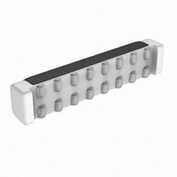
RES-NET 47K OHM BUSSED SMD
Manufacturer
CTS Resistor Products
Series
752r
Specifications of 752161473GPTR
Resistance (ohms)
47K
Number Of Resistors
14
Circuit Type
Bussed
Temperature Coefficient
±200ppm/°C
Tolerance
±2%
Power Per Element
80mW
Number Of Pins
16
Package / Case
16-DRT
Size / Dimension
0.465" L x 0.080" W (11.81mm x 2.03mm)
Height
0.095" (2.41mm)
Mounting Type
Surface Mount
Operating Temperature
-55°C ~ 125°C
Lead Free Status / RoHS Status
Lead free / RoHS Compliant
Other names
752-161-47KPTR


Application Information
GENERAL MIXED-SIGNAL LAYOUT
RECOMMENDATION
This section provides practical guidelines for mixed signal
PCB layout that involves various digital/analog power and
ground traces. Designers should note that these are only
"rule-of-thumb" recommendations and the actual results will
depend heavily on the final layout.
Power and Ground Circuits
For 2 layer mixed signal design, it is important to isolate the
digital power and ground trace paths from the analog power
and ground trace paths. Star trace routing techniques (bring-
ing individual traces back to a central point rather than daisy
chaining traces together in a serial manner) can have a
major impact on low level signal performance. Star trace
routing refers to using individual traces to feed power and
ground to each circuit or even device. This technique will
take require a greater amount of design time but will not
increase the final price of the board. The only extra parts
required may be some jumpers.
FIGURE 3. Demo Board Reference Schematic
(Continued)
15
Single-Point Power / Ground Connection
The analog power traces should be connected to the digital
traces through a single point (link). A "Pi-filter" can be helpful
in minimizing high frequency noise coupling between the
analog and digital sections. It is further recommended to
place digital and analog power traces over the correspond-
ing digital and analog ground traces to minimize noise cou-
pling.
Placement of Digital and Analog Components
All digital components and high-speed digital signals traces
should be located as far away as possible from analog
components and circuit traces.
Avoiding Typical Design / Layout Problems
Avoid ground loops or running digital and analog traces
parallel to each other (side-by-side) on the same PCB layer.
When traces must cross over each other do it at 90 degrees.
Running digital and analog traces at 90 degrees to each
other from the top to the bottom side as much as possible will
minimize capacitive noise coupling and crosstalk.
20126250
www.national.com
Related parts for 752161473GPTR
Image
Part Number
Description
Manufacturer
Datasheet
Request
R

Part Number:
Description:
RESISTOR NET 4.7K OHM SMD
Manufacturer:
CTS Resistor Products
Datasheet:

Part Number:
Description:
RES .10 OHM 1/8W 5% 0805
Manufacturer:
CTS Resistor Products
Datasheet:

Part Number:
Description:
RES .20 OHM 1/10W 5% 0402
Manufacturer:
CTS Resistor Products
Datasheet:

Part Number:
Description:
RES .47 OHM 1/8W 5% 0805
Manufacturer:
CTS Resistor Products
Datasheet:

Part Number:
Description:
RES .47 OHM 1/10W 5% 0402
Manufacturer:
CTS Resistor Products
Datasheet:

Part Number:
Description:
RES .47 OHM 1/4W 5% 1206
Manufacturer:
CTS Resistor Products
Datasheet:

Part Number:
Description:
RES .20 OHM 1/10W 5% 0603
Manufacturer:
CTS Resistor Products
Datasheet:

Part Number:
Description:
RES .47 OHM 1/2W 5% 1210
Manufacturer:
CTS Resistor Products
Datasheet:

Part Number:
Description:
RES .20 OHM 1/2W 5% 1210
Manufacturer:
CTS Resistor Products
Datasheet:

Part Number:
Description:
RES .47 OHM .75W 5% 2010
Manufacturer:
CTS Resistor Products
Datasheet:

Part Number:
Description:
RES .20 OHM .75W 5% 2010
Manufacturer:
CTS Resistor Products
Datasheet:

Part Number:
Description:
RES .56 OHM .75W 5% 2010
Manufacturer:
CTS Resistor Products
Datasheet:

Part Number:
Description:
RES .91 OHM .75W 5% 2010
Manufacturer:
CTS Resistor Products
Datasheet:

Part Number:
Description:
RES .050 OHM .5W 5% 1206
Manufacturer:
CTS Resistor Products
Datasheet:

Part Number:
Description:
RES NET 15RES 4.7K OHM 16PIN SMD
Manufacturer:
CTS Resistor Products
Datasheet: