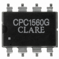
CPC1560GSTR Clare, CPC1560GSTR Datasheet - Page 9

CPC1560GSTR
Manufacturer Part Number
CPC1560GSTR
Description
RELAY OPTOMOS SP-NO 600MA 8-SMD
Manufacturer
Clare
Series
CPC, OptoMOS®r
Datasheet
1.CPC1560GSTR.pdf
(14 pages)
Specifications of CPC1560GSTR
Circuit
SPST-NO (1 Form A)
Output Type
AC, DC
On-state Resistance
5.6 Ohm
Load Current
600mA
Voltage - Input
1.22VDC
Voltage - Load
0 ~ 60 V
Mounting Type
Surface Mount
Termination Style
Gull Wing
Package / Case
8-SMD (300 mil)
Lead Free Status / RoHS Status
Lead free / RoHS Compliant
Other names
CLA305TR
Available stocks
Company
Part Number
Manufacturer
Quantity
Price
Company:
Part Number:
CPC1560GSTR
Manufacturer:
CIRRUS
Quantity:
1 439
4.2 Storage Capacitor
The CPC1560 requires the use of an external
capacitor (C
This external storage capacitor enables the relay to
turn on quickly by holding a reservoir of charge to be
transferred to the gates of the MOSFET pair. The
capacitor must have a minimum working voltage
greater than the load voltage, and must be connected
from pin 8 (C+), the capacitor’s positive voltage
terminal, to pin 5 (C-), the capacitor’s negative voltage
terminal.
Proper selection of the external capacitor begins with
the recommended range provided in the
“Recommended Operating Conditions” on page
maximum voltage at the CPC1560 outputs, including
transients and faults. The nominal value of the
capacitor needs to be chosen so that when the effects
of tolerance, temperature coefficient, and (for some
types of capacitor) derating due to bias voltage are
accounted for, the capacitor’s value remains within the
recommended range over the operational conditions
of the end product.
5. Operational Behavior
5.1 Operating Frequency
Equation 1 shows the relationship between power
dissipation, operating frequency, and duty cycle for the
CPC1560 device. From this equation, it can be seen
that both switching frequency (f
(D) contribute to power dissipation. The first one by
generating switching losses, and the second one by
generating ON losses. Switching losses are those
caused by changes in the energy state of the load
components when the device is switching on and off
(i.e. E
caused by the flow of current (I
on-resistance (R
(1) P
Because a higher operating frequency translates into
higher power consumed by the part, care must be
taken to limit its value in order to protect the device
from exceeding its maximum power rating. When
doing this, both the maximum allowed power
dissipation in the part and the ON duty cycle,
D=t
R00F
ON
5.1.1 Duty Cycle/Power Dissipation
avg
RISE
/ (t
= I
ON
and E
L
EXT
2
+t
• R
OFF
) to meet the device’s specifications.
ON
ON
FALL
), must be taken into consideration.
) when it is switched on.
• D + f
), and ON losses are those
switch
• (E
L
switch
) through the part’s
RISE
) and duty cycle
+ E
FALL
4, and the
)
PRELIMINARY
When setting the operating frequency of the
CPC1560, the user must also take into account power
dissipation over temperature.
In addition to ambient temperature, the maximum
frequency of the CPC1560 is also determined by the
MOSFET’s turn-on and turn-off times and the load
voltage rise and fall times as follows:
Where 1/3 is a multiplication factor for temperature
and process variations.
5.2 Switching Losses
During the transition intervals of the switching process,
the load components change energy states, which
results in switching losses as the energy passes
through the MOSFETs. This energy transfer is
manifested in the form of heat dissipation and must be
taken into consideration.
Energy is transferred during the turn-off intervals. This
energy, called E
output switches, and if present parasitic load
capacitance and the protection device.
Energy is also transferred during the turn-on intervals
and is called E
MOSFET output switches, which is why this energy
should be limited to the “peak turn-on energy” values
specified in the Absolute Maximum Ratings Table of
this datasheet.
The user of the CPC1560 device must understand the
details of the load behavior and keep in mind the
device’s recommended operating conditions in order
to adequately size the load components and protect
the application circuit.
The average power of the CPC1560 output MOSFET
for any specific application and for any load type given
by Equation 1 and repeated here is:
From this equation we can see how the switching
losses (E
losses,” contribute to the CPC1560’s output power
dissipation.
The user must also know that the recommended
operating conditions for I
(3) P
(2)
5.1.2 Temperature Effects
5.1.3 Elements of Operating Frequency
avg
f
MAX
= I
RISE
L
2
=
• R
and E
fall
1
3
rise
ON
. This energy will be absorbed by the
(t
, will be absorbed by the MOSFET
ON
• D + f
FALL
+ t
), together with the “on
L
OFF
switch
, f
SWITCH
)
-1
• (E
RISE
, load capacitance
+ E
FALL
CPC1560
)
9


