DEMO9S08QG8 Freescale Semiconductor, DEMO9S08QG8 Datasheet - Page 9
DEMO9S08QG8
Manufacturer Part Number
DEMO9S08QG8
Description
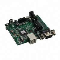
BOARD EVAL FOR MC9S08QG4/8
Manufacturer
Freescale Semiconductor
Datasheet
1.DEMO9S08QG8.pdf
(18 pages)
Specifications of DEMO9S08QG8
Lead Free Status / RoHS Status
Contains lead / RoHS non-compliant
Available stocks
Company
Part Number
Manufacturer
Quantity
Price
Company:

Part Number:
DEMO9S08QG8E
Manufacturer:
Freescale Semiconductor
Quantity:
135


Power may be sourced to off-board circuitry through the J1 connector. The current limitation of
the USB bus or the on-board regulator must be considered when attempting to source power
to external circuitry. Excessive current drain may damage the target board, the host PC USB
hub, or the on-board regulator. The figure below details the VX_EN option header
connections.
Figure 2. VX_EN Option Header
RESET SWITCH
The RESET switch provides a method to apply an asynchronous reset to the MCU and is
connected directly to the PTA5/RESET* input on the MCU. Pressing the RESET switch forces
the MCU RESET* input low. The MC9S08QG8 MCU applies an internal pull-up on the
RESET* line to prevent spurious resets and allow normal operation.
LOW VOLTAGE DETECT
The MC9S08QG8 utilizes an internal Low Voltage Detect (LVD) to protect against under-
voltage conditions. The LVD is enabled out of RESET. Consult the MC9S08QG8 Device User
Guide for details on configuring LVD operation.
STOP MODES
The MC9S08QG8 can be configured for three different low power stop modes. If stop1 or
stop2 modes are entered, an external pull-up resistor must be placed between the
PTA5/RESET*/IRQ*/TCLK pin and VDD. This pull-up resistor is not included on the
APS08QG8SLK board. If these modes will be used with this board, a 10K – 50K ohm resistor
can be placed between pins J1-1 and J1-2 to ensure proper operation of the MCU. The
jumper for the VX_EN header must also be in place in this case. Consult the MC9S08QG8
Device User Guide for more details on configuring the low power stop modes.
TIMING
By default, the APS08QG8SLK uses timing provided from an internal 32 kHz frequency
reference and an internal frequency-locked loop (FLL). The FLL output is trimmable to ± 0.2%
Freescale Semiconductor
CAUTION: Do not apply power to connector J1 while also sourcing power from either the PWR
NOTE: Do not exceed available current supply from the USB-BDM cable or on-board regulator
VX_EN
VX_EN
▪
▪
when sourcing power through connector J1 to external circuitry.
connector or the USB-BDM circuit. Damage to the board may result.
OFF
ON
Enable power connection to connector J1
Disable power connection to connector J1
9
Related parts for DEMO9S08QG8
Image
Part Number
Description
Manufacturer
Datasheet
Request
R

Part Number:
Description:
Manufacturer:
STMicroelectronics
Datasheet:

Part Number:
Description:
DEMO BOARD FOR HMC6042/HMC1041Z
Manufacturer:
Honeywell Microelectronics & Precision Sensors

Part Number:
Description:
DEMO BOARD FOR HMC1042L/HMC1041Z
Manufacturer:
Honeywell Microelectronics & Precision Sensors
Datasheet:

Part Number:
Description:
KIT DEMO 4 SENSOR CHAN RS232
Manufacturer:
VTI Technologies
Datasheet:


Part Number:
Description:
DEMO: DC Power Supply, 32 Volts, 3 Amps
Manufacturer:
Tektronix
Part Number:
Description:
DEMO: Programmable DC Power Supply, 32 Volts, 3 Amps
Manufacturer:
Tektronix

Part Number:
Description:
Manufacturer:
Freescale Semiconductor, Inc
Datasheet:
Part Number:
Description:
Manufacturer:
Freescale Semiconductor, Inc
Datasheet:
Part Number:
Description:
Manufacturer:
Freescale Semiconductor, Inc
Datasheet:
Part Number:
Description:
Manufacturer:
Freescale Semiconductor, Inc
Datasheet:
Part Number:
Description:
Manufacturer:
Freescale Semiconductor, Inc
Datasheet:
Part Number:
Description:
Manufacturer:
Freescale Semiconductor, Inc
Datasheet:
Part Number:
Description:
Manufacturer:
Freescale Semiconductor, Inc
Datasheet:
Part Number:
Description:
Manufacturer:
Freescale Semiconductor, Inc
Datasheet: