MPC566EVB Freescale Semiconductor, MPC566EVB Datasheet - Page 50
MPC566EVB
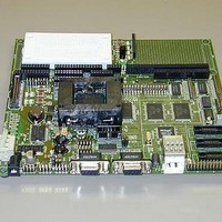
Manufacturer Part Number
MPC566EVB
Description
KIT EVALUATION FOR MPC565/566
Manufacturer
Freescale Semiconductor
Specifications of MPC566EVB
Processor To Be Evaluated
MPC56x
Data Bus Width
32 bit
Interface Type
RS-232, Ethernet
Lead Free Status / RoHS Status
Contains lead / RoHS non-compliant


1
System Power-up and Initial Operation
RW0, RW2, RW4 – 18, RW23 – 30 provide the user access to external Reset Configuration Word
(RCW) bits not normally required for default MPC566EVB operation. The RW0 – 30 designations
reflect the data bus D0 – D30 bit affected when the RCW word is enabled externally. All RW0 –
30 option bits are defaulted to the logic low value during external RCW word operation. The user
may apply a wire jumper between the 2 pad positions of each RW0 – 30 option to provide a logic
high level on the respective bit position during external RCW operation. Note that the user could
add physical headers (2mm type) to these signals on the board. Refer to the MPC566 user manual
Reset chapter for the respective RCW bit definitions.
2.3.2 Memory Configuration (MAP_SW)
The Memory Configuration switch (MAP_SW) controls the mapping of the MPC566 chip selects
to the different external memories and whether the internal flash is enabled.I
2.4 System Power-up and Initial Operation
When all of the cables are connected to the board, power may be applied. The dBUG ROM Monitor
initializes the board and then displays a power-up message on the terminal.
Part Number: 0xXX
MaskNum: 0xXX
Copyright 1995-2002 Motorola, Inc.
MPC566 MPC566EVB Firmware v3b.1a.xx (Build XXX on XXX
xx:xx:xx)
Enter 'help' for help.
2-10
Switch
Each Chip Select should only be connected to one device.
1
2
3
4
5
6
7
8
CS3-TA
Name
CS0
CS1
CS0
CS2
CS3
2.6v
IP
1
1
1
1
1
100_CS/LCD_
MPC565/566
Function
RAM_CS
RAM_CS
RCW-IP
FL_CS
FL_CS
FLEN
CS
Freescale Semiconductor, Inc.
TA
For More Information On This Product,
MPC566EVB User’s Manual
TA for LCD or Connect the EtherNet Controller TA to the Pro-
Go to: www.freescale.com
Table 2-4. MAP_SW
CS3 connected to the Ethernet and LCD Interface
All Rights Reserved.
CS0 connected to the External SRAM
CS1 connected to the External SRAM
CS0 connected to the External Flash
CS1 connected to the External Flash
Enable Internal MPC565/566 Flash
Switch Closed
IP bit is set
cessor TA
XX 20XX
Default
off
on
on
off
on
on
on
off
Related parts for MPC566EVB
Image
Part Number
Description
Manufacturer
Datasheet
Request
R

Part Number:
Description:
Manufacturer:
Freescale Semiconductor, Inc
Datasheet:
Part Number:
Description:
Manufacturer:
Freescale Semiconductor, Inc
Datasheet:
Part Number:
Description:
Manufacturer:
Freescale Semiconductor, Inc
Datasheet:
Part Number:
Description:
Manufacturer:
Freescale Semiconductor, Inc
Datasheet:
Part Number:
Description:
Manufacturer:
Freescale Semiconductor, Inc
Datasheet:
Part Number:
Description:
Manufacturer:
Freescale Semiconductor, Inc
Datasheet:
Part Number:
Description:
Manufacturer:
Freescale Semiconductor, Inc
Datasheet:
Part Number:
Description:
Manufacturer:
Freescale Semiconductor, Inc
Datasheet:
Part Number:
Description:
Manufacturer:
Freescale Semiconductor, Inc
Datasheet:
Part Number:
Description:
Manufacturer:
Freescale Semiconductor, Inc
Datasheet:
Part Number:
Description:
Manufacturer:
Freescale Semiconductor, Inc
Datasheet:
Part Number:
Description:
Manufacturer:
Freescale Semiconductor, Inc
Datasheet:
Part Number:
Description:
Manufacturer:
Freescale Semiconductor, Inc
Datasheet:
Part Number:
Description:
Manufacturer:
Freescale Semiconductor, Inc
Datasheet:
Part Number:
Description:
Manufacturer:
Freescale Semiconductor, Inc
Datasheet: