C8051F040DK-U Silicon Laboratories Inc, C8051F040DK-U Datasheet - Page 9
C8051F040DK-U
Manufacturer Part Number
C8051F040DK-U
Description
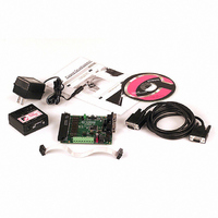
DEV KIT FOR F040/F041/F042/F043
Manufacturer
Silicon Laboratories Inc
Datasheet
1.C8051F040DK.pdf
(16 pages)
Specifications of C8051F040DK-U
Lead Free Status / RoHS Status
Contains lead / RoHS non-compliant
Other names
336-1050
C8051F04DK-U
C8051F04DK-U


6.4. Serial Interface (J5)
A RS232 transceiver circuit and DB-9 (J5) connector are provided on the target board to facilitate serial connec-
tions to UART0 of the C8051F040. The TX, RX, RTS and CTS signals of UART0 may be connected to the DB-9
connector and transceiver by installing shorting blocks on headers J6, J8, J9 and J10.
6.5. Analog I/O (J11, J20)
Several C8051F040 analog signals are routed to the J20 terminal block and the J11 header. The J11 connector
provides the ability to connect DAC0 and DAC1 outputs to several different analog inputs by installing a shorting
block between a DAC output and an analog input on adjacent pins of J11. Refer to Table 3 for J20 terminal block
connections and Table 4 for J11 pin definitions.
J6 - Install shorting block to connect UART0 TX (P0.0) to transceiver.
J9 - Install shorting block to connect UART0 RX (P0.1) to transceiver.
J8 - Install shorting block to connect UART0 RTS (P4.0) to transceiver.
J10 - Install shorting block to connect UART0 CTS (P4.1) to transceiver.
Table 3. J20 Terminal Block Pin Descriptions
Table 4. J11 Connector Pin Descriptions
Pin #
Pin #
1
2
3
4
5
6
7
8
1
2
3
4
5
6
ADND (Analog Ground)
Rev. 0.6
Description
Description
HVAIN+
HVREF
HVAIN-
VREF0
AIN0.0
AIN0.1
AIN0.0
AIN0.1
AIN0.2
AIN0.3
DAC1
DAC0
DAC1
C8051F04x-DK
9
Related parts for C8051F040DK-U
Image
Part Number
Description
Manufacturer
Datasheet
Request
R

Part Number:
Description:
SMD/C°/SINGLE-ENDED OUTPUT SILICON OSCILLATOR
Manufacturer:
Silicon Laboratories Inc
Part Number:
Description:
Manufacturer:
Silicon Laboratories Inc
Datasheet:
Part Number:
Description:
N/A N/A/SI4010 AES KEYFOB DEMO WITH LCD RX
Manufacturer:
Silicon Laboratories Inc
Datasheet:
Part Number:
Description:
N/A N/A/SI4010 SIMPLIFIED KEY FOB DEMO WITH LED RX
Manufacturer:
Silicon Laboratories Inc
Datasheet:
Part Number:
Description:
N/A/-40 TO 85 OC/EZLINK MODULE; F930/4432 HIGH BAND (REV E/B1)
Manufacturer:
Silicon Laboratories Inc
Part Number:
Description:
EZLink Module; F930/4432 Low Band (rev e/B1)
Manufacturer:
Silicon Laboratories Inc
Part Number:
Description:
I°/4460 10 DBM RADIO TEST CARD 434 MHZ
Manufacturer:
Silicon Laboratories Inc
Part Number:
Description:
I°/4461 14 DBM RADIO TEST CARD 868 MHZ
Manufacturer:
Silicon Laboratories Inc
Part Number:
Description:
I°/4463 20 DBM RFSWITCH RADIO TEST CARD 460 MHZ
Manufacturer:
Silicon Laboratories Inc
Part Number:
Description:
I°/4463 20 DBM RADIO TEST CARD 868 MHZ
Manufacturer:
Silicon Laboratories Inc
Part Number:
Description:
I°/4463 27 DBM RADIO TEST CARD 868 MHZ
Manufacturer:
Silicon Laboratories Inc
Part Number:
Description:
I°/4463 SKYWORKS 30 DBM RADIO TEST CARD 915 MHZ
Manufacturer:
Silicon Laboratories Inc
Part Number:
Description:
N/A N/A/-40 TO 85 OC/4463 RFMD 30 DBM RADIO TEST CARD 915 MHZ
Manufacturer:
Silicon Laboratories Inc
Part Number:
Description:
I°/4463 20 DBM RADIO TEST CARD 169 MHZ
Manufacturer:
Silicon Laboratories Inc