C8051F040DK-U Silicon Laboratories Inc, C8051F040DK-U Datasheet - Page 8
C8051F040DK-U
Manufacturer Part Number
C8051F040DK-U
Description
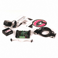
DEV KIT FOR F040/F041/F042/F043
Manufacturer
Silicon Laboratories Inc
Datasheet
1.C8051F040DK.pdf
(16 pages)
Specifications of C8051F040DK-U
Lead Free Status / RoHS Status
Contains lead / RoHS non-compliant
Other names
336-1050
C8051F04DK-U
C8051F04DK-U


C8051F04x-DK
6.1. System Clock Sources
The C8051F040 device installed on the target board features a calibrated programmable internal oscillator which is
enabled as the system clock source on reset. After reset, the internal oscillator operates at a frequency of
3.0625 MHz (±2%) by default but may be configured by software to operate at other frequencies. Therefore, in many
applications an external oscillator is not required. However, an external 22.1184 MHz crystal is installed on the target
board for additional applications. Refer to the C8051F04x data sheet for more information on configuring the system
clock source.
6.2. Switches and LEDs
Two switches are provided on the target board. Switch SW1 is connected to the RESET pin of the C8051F040.
Pressing SW1 puts the device into its hardware-reset state. Switch SW2 is connected to the C8051F040’s general
purpose I/O (GPIO) pin through headers. Pressing SW2 generates a logic low signal on the port pin. Remove the
shorting block from the header to disconnect SW2 from the port pins. The port pin signal is also routed to a pin on
the J24 I/O connector. See Table 1 for the port pins and headers corresponding to each switch.
Two LEDs are also provided on the target board. The red LED labeled PWR is used to indicate a power connection
to the target board. The green LED labeled with a port pin name is connected to the C8051F040’s GPIO pin
through headers. Remove the shorting block from the header to disconnect the LED from the port pin. The port pin
signal is also routed to a pin on the J24 I/O connector. See Table 1 for the port pins and headers corresponding to
each LED.
6.3. Target Board JTAG Interface (J4)
The JTAG connector (J4) provides access to the JTAG pins of the C8051F040. It is used to connect the Serial
Adapter or the USB Debug Adapter to the target board for in-circuit debugging and Flash programming. Table 2
shows the JTAG pin definitions.
8
Table 2. JTAG Connector Pin Descriptions
Table 1. Target Board I/O Descriptions
Description
Green LED
Red LED
2, 3, 9
Pin #
SW1
SW2
8, 10
1
4
5
6
7
+3 VD (+3.3 VDC)
Rev. 0.6
Reset
Not Connected
GND (Ground)
PWR
P3.7
P1.6
Description
I/O
TCK
TMS
TDO
TDI
Header
none
none
J1
J3
Related parts for C8051F040DK-U
Image
Part Number
Description
Manufacturer
Datasheet
Request
R

Part Number:
Description:
SMD/C°/SINGLE-ENDED OUTPUT SILICON OSCILLATOR
Manufacturer:
Silicon Laboratories Inc
Part Number:
Description:
Manufacturer:
Silicon Laboratories Inc
Datasheet:
Part Number:
Description:
N/A N/A/SI4010 AES KEYFOB DEMO WITH LCD RX
Manufacturer:
Silicon Laboratories Inc
Datasheet:
Part Number:
Description:
N/A N/A/SI4010 SIMPLIFIED KEY FOB DEMO WITH LED RX
Manufacturer:
Silicon Laboratories Inc
Datasheet:
Part Number:
Description:
N/A/-40 TO 85 OC/EZLINK MODULE; F930/4432 HIGH BAND (REV E/B1)
Manufacturer:
Silicon Laboratories Inc
Part Number:
Description:
EZLink Module; F930/4432 Low Band (rev e/B1)
Manufacturer:
Silicon Laboratories Inc
Part Number:
Description:
I°/4460 10 DBM RADIO TEST CARD 434 MHZ
Manufacturer:
Silicon Laboratories Inc
Part Number:
Description:
I°/4461 14 DBM RADIO TEST CARD 868 MHZ
Manufacturer:
Silicon Laboratories Inc
Part Number:
Description:
I°/4463 20 DBM RFSWITCH RADIO TEST CARD 460 MHZ
Manufacturer:
Silicon Laboratories Inc
Part Number:
Description:
I°/4463 20 DBM RADIO TEST CARD 868 MHZ
Manufacturer:
Silicon Laboratories Inc
Part Number:
Description:
I°/4463 27 DBM RADIO TEST CARD 868 MHZ
Manufacturer:
Silicon Laboratories Inc
Part Number:
Description:
I°/4463 SKYWORKS 30 DBM RADIO TEST CARD 915 MHZ
Manufacturer:
Silicon Laboratories Inc
Part Number:
Description:
N/A N/A/-40 TO 85 OC/4463 RFMD 30 DBM RADIO TEST CARD 915 MHZ
Manufacturer:
Silicon Laboratories Inc
Part Number:
Description:
I°/4463 20 DBM RADIO TEST CARD 169 MHZ
Manufacturer:
Silicon Laboratories Inc