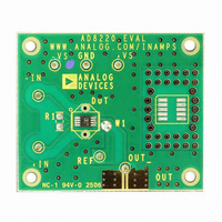
AD8220-EVALZ Analog Devices Inc, AD8220-EVALZ Datasheet
AD8220-EVALZ
Specifications of AD8220-EVALZ
AD8220-EVAL


Related parts for AD8220-EVALZ


AD8220-EVALZ Summary of contents
Page 1
... Despite the JFET inputs, the AD8220 typically has a noise corner of only 10 Hz. With the proliferation of mixed-signal processing, the number of power supplies required in each system has grown. The AD8220 is designed to alleviate this problem. The AD8220 can operate on a ± ...
Page 2
... AD8220 TABLE OF CONTENTS Features .............................................................................................. 1 Applications ....................................................................................... 1 Pin Configuration ............................................................................. 1 General Description ......................................................................... 1 Revision History ............................................................................... 2 Specifications ..................................................................................... 3 Absolute Maximum Ratings ............................................................ 8 ESD Caution .................................................................................. 8 Pin Configuration and Function Descriptions ............................. 9 Typical Performance Characteristics ........................................... 10 Theory of Operation ...................................................................... 19 Gain Selection ............................................................................. 20 Layout ........................................................................................... 20 Reference Terminal .................................................................... 21 REVISION HISTORY 5/10—Rev Rev. B Added W Grade .................................................................. Universal Changes to Features Section and General Description Section . 1 Changes to Specifications Section and Table 1 ...
Page 3
... AD8220 Unit nV/√Hz nV/√Hz μV p-p μV p-p fA/√Hz μV μV/°C μV μV/° kHz kHz kHz kHz ...
Page 4
... AD8220 Parameter Test Conditions Settling Time 0.01 step 100 G = 1000 Settling Time 0.001 step 100 G = 1000 Slew Rate 100 T A GAIN (49.4 kΩ/R T for A, B grades for W grade OPR Gain Range Gain Error V = ±10 V OUT 100 G = 1000 Gain Nonlinearity V = OUT − ...
Page 5
... Differential and common-mode input impedance can be calculated from the pin impedance The AD8220 can operate diode drop below the negative supply but the bias current increases sharply. The input voltage range reflects the maximum allowable voltage where the input bias current is within the specification. ...
Page 6
... AD8220 Parameter Test Conditions INPUT CURRENT Input Bias Current T A Over Temperature T OPR Input Offset Current T A Over Temperature T OPR DYNAMIC RESPONSE T A Small Signal Bandwidth, − 100 G = 1000 Settling Time 0.01 step step G = 100 4 V step G = 1000 4 V step Settling Time 0.001% ...
Page 7
... Differential and common-mode impedance can be calculated from the pin impedance The AD8220 can operate diode drop below the negative supply but the bias current increases sharply. The input voltage range reflects the maximum allowable voltage where the input bias current is within the specification. ...
Page 8
... AD8220 ABSOLUTE MAXIMUM RATINGS Table 3. Parameter Supply Voltage Power Dissipation Output Short-Circuit Current Input Voltage (Common Mode) Differential Input Voltage Storage Temperature Range 2 Operating Temperature Range Lead Temperature (Soldering 10 sec) Junction Temperature θ (4-Layer JEDEC Standard Board) JA Package Glass Transition Temperature ...
Page 9
... Negative Power Supply Terminal S 6 REF Reference Voltage Terminal (Drive This Terminal with a Low Impedance Voltage Source to Level-Shift the Output Output Terminal OUT 8 +V Positive Power Supply Terminal S AD8220 – OUT R REF + –V S TOP VIEW (Not to Scale) Figure 4. Pin Configuration Pins) G Rev Page AD8220 ...
Page 10
... AD8220 TYPICAL PERFORMANCE CHARACTERISTICS 1200 1000 800 600 400 200 0 –40 –20 0 CMRR (µV/V) Figure 5. Typical Distribution of CMRR ( 1000 800 600 400 200 0 –200 –100 0 V (µV) OSI Figure 6. Typical Distribution of Input Offset Voltage 1000 800 600 400 200 0 –1000 –500 ...
Page 11
... Figure 15. Negative PSRR vs. Frequency, RTI INPUT OFFSET 9 CURRENT ± –15.1V 3 –5.1V 1 –1 1k –16 –12 Figure 16. Input Bias Current and Input Offset Current vs. Rev Page AD8220 GAIN = 1000 BANDWIDTH LIMITED GAIN = 10 GAIN = 1 10 100 1k 10k 100k FREQUENCY (Hz) GAIN = 1000 GAIN = 10 GAIN = 100 10 ...
Page 12
... AD8220 10n 1n I BIAS 100p 10p 1p 0.1p –50 – TEMPERATURE (°C) Figure 17. Input Bias Current and Offset Current vs. Temperature ± REF 10n 1n I BIAS 100p 10p 1p 0.1p –50 – TEMPERATURE (°C) Figure 18. Input Bias Current and Offset Current vs. Temperature 2 REF 160 ...
Page 13
... Figure 27. Input Common-Mode Voltage Range vs. Output Voltage –1 – Figure 28. Input Common-Mode Voltage Range vs. Output Voltage, Rev Page AD8220 R = 2kΩ LOAD R = 10kΩ LOAD = ±15V –8 –6 –4 – OUTPUT VOLTAGE (V) Figure 26. Gain Nonlinearity 1000 +13V ± ...
Page 14
... OUTPUT VOLTAGE (V) Figure 30. Input Common-Mode Voltage Range vs. Output Voltage 100 2 REF –1 +125°C –40°C –2 +25°C NOTES 1. THE AD8220 CAN OPERATE THE NEGATIVE SUPPLY, BUT THE BIAS CURRENT WILL INCREASE SHARPLY. +1 –40°C +25°C +85°C +125°C V – S – ...
Page 15
... Figure 40. Output Voltage Swing vs. Large Signal Frequency Response = 2 REF Rev Page 47pF NO LOAD 100pF 20mV/DIV 5µs/DIV XX XX XXX ( ± REF XX 47pF 100pF NO LOAD 20mV/DIV 5µs/DIV XX XX XXX ( 2 REF 35 GAIN = 10, 100, 1000 30 GAIN = 100 1k 10k 100k FREQUENCY (Hz) AD8220 10M ...
Page 16
... AD8220 XX 5V/DIV 5µs TO 0.01% 6µs TO 0.001% 0.002%/DIV XX XX XXX (X) Figure 41. Large Signal Pulse Response and Settle Time kΩ ± LOAD S XX 5V/DIV 4.3μs TO 0.01% 0.002%/DIV 4.6μs TO 0.001 XXX (X) Figure 42. Large Signal Pulse Response and Settle Time 10 kΩ ...
Page 17
... C = 100 pF, LOAD LOAD Rev Page 20mV/DIV XXX = 2 kΩ, C LOAD 2 REF 20mV/DIV XXX = 2 kΩ, C LOAD 2 REF 20mV/DIV XXX Figure 52. Small Signal Pulse Response 1000 100 pF 2.5 V LOAD S REF AD8220 4µs/DIV = 100 pF, LOAD 4µs/DIV = 100 pF, LOAD 40µs/DIV = 2 kΩ, LOAD ...
Page 18
... AD8220 15 10 SETTLED TO 0.001% 5 SETTLED TO 0.01 OUTPUT VOLTAGE STEP SIZE (V) Figure 53. Settling Time vs. Output Voltage Step Size ( ± 100 Figure 54. Settling Time vs. Gain for Step, V REF Rev Page SETTLED TO 0.001% SETTLED TO 0.01% 10 100 1000 GAIN (V/V) = ± REF ...
Page 19
... AD8220 gain-bandwidth product increases with gain, resulting in a system that does not suffer as much bandwidth loss as voltage feedback architectures at higher gains. A unique pinout enables the AD8220 to meet a CMRR specification through 5 kHz (G = 1). The balanced pinout, shown in Figure 56, reduces parasitics that adversely affect CMRR performance ...
Page 20
... The AD8220 defaults when no gain resistor is used. Gain accuracy is determined by the absolute tolerance of R The TC of the external gain resistor increases the gain drift of the instrumentation amplifier. Gain error and gain drift are kept to a minimum when the gain resistor is not used. ...
Page 21
... S Figure 59. Supply Decoupling, REF and Output Referred to Ground INPUT BIAS CURRENT RETURN PATH The AD8220 input bias current is extremely small at less than 10 pA. Nonetheless, the input bias current must have a return path to common. When the source, such as a transformer, cannot provide a return current path, one should be created (see Figure 60) ...
Page 22
... RF INTERFERENCE RF rectification is often a problem in applications where there are large RF signals. The problem appears as a small dc offset voltage. The AD8220 by its nature has gate capacitance, C inputs. Matched series resistors form a natural low-pass filter that reduces rectification at high frequency (see Figure 61). The relationship between external, matched series resistors and the ...
Page 23
... In other cases, transmission over a long distance can require differential processing for better immunity to interference. Figure 65 shows how to configure the AD8220 to output a differential signal. An OP1177 op amp is used to create a differential voltage. Errors from the op amp are common to both outputs and are thus common mode. Likewise, errors from using mismatched resistors cause a common-mode dc offset error ...
Page 24
... AD8220 AMPLITUDE +5V TIME –5V ±5V 0.1µF TIME +IN ±5V –IN 0.1µF +5V 10µF Figure 66. Configuring the AD8220 to Output A Ratiometric, Differential Signal +15V 0.1µF +IN AD8220 REF 4.99kΩ –IN 0.1µF –15V –15V OP1177 +5V 4.99kΩ 0.1µF 10µF Figure 65. Differential Output with Level Shift ...
Page 25
... ECGs. Figure 67 shows an example ECG schematic. Following the AD8220 is a 0.033 Hz high-pass filter, formed by the 4.7 μF capacitor and the 1 MΩ resistor, which removes the dc offset that develops between the electrodes. An additional gain of 50, provided by the AD8618, makes use of the input range of the ADC ...
Page 26
... See the Typical Performance Characteristics section for expected operation from 85°C to 125°C. AUTOMOTIVE PRODUCTS The AD8220W models are available with controlled manufacturing to support the quality and reliability requirements of automotive applications. Note that these automotive models may have specifications that differ from the commercial models; therefore, designers should review the Specifications section of this data sheet carefully ...
Page 27
... NOTES Rev Page AD8220 ...
Page 28
... AD8220 NOTES ©2006–2010 Analog Devices, Inc. All rights reserved. Trademarks and registered trademarks are the property of their respective owners. D03579-0-5/10(B) Rev Page ...