EVAL-ADF4112EB1 Analog Devices Inc, EVAL-ADF4112EB1 Datasheet - Page 2
EVAL-ADF4112EB1
Manufacturer Part Number
EVAL-ADF4112EB1
Description
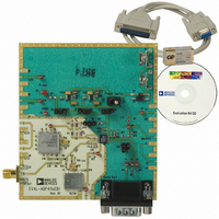
BOARD EVAL FOR ADF4112
Manufacturer
Analog Devices Inc
Type
Frequency Synthesizerr
Datasheet
1.ADF4113BRUZ.pdf
(28 pages)
Specifications of EVAL-ADF4112EB1
Contents
Evaluation Board
For Use With/related Products
ADF4112
Lead Free Status / RoHS Status
Contains lead / RoHS non-compliant


ADF4110/ADF4111/ADF4112/ADF4113
TABLE OF CONTENTS
Specifications..................................................................................... 3
Timing Characteristics..................................................................... 5
Absolute Maximum Ratings............................................................ 6
Pin Configurations and Function Descriptions ........................... 7
Typical Performance Characteristics ............................................. 8
Circuit Description......................................................................... 12
REVISION HISTORY
3/04—Data sheet changed from Rev. B to Rev. C.
Updated Format..............................................................Universal
Changes to Specifications ............................................................ 2
Changes to Figure 32.................................................................. 22
Changes to the Ordering Guide................................................ 28
3/03—Data sheet changed from Rev. A to Rev. B.
Edits to Specifications .................................................................. 2
Updated OUTLINE DIMENSIONS ........................................ 24
1/01—Data sheet changed from Rev. 0 to Rev. A.
Changes to DC Specifications in B Version, B Chips,
Changes to Absolute Maximum Rating..................................... 4
Changes to FR
Changes to Figure 8...................................................................... 7
New Graph Added—TPC 22....................................................... 9
Change to PD Polarity Box in Table V..................................... 15
Change to PD Polarity Box in Table VI ................................... 16
Change to PD Polarity Paragraph ............................................ 17
Addition of New Material
Replacement of CP-20 Outline with CP-20 [2] Outline........ 24
Transistor Count........................................................................... 6
ESD Caution.................................................................................. 6
Reference Input Section............................................................. 12
RF Input Stage............................................................................. 12
Prescaler (P/P + 1)...................................................................... 12
A and B Counters ....................................................................... 12
R Counter .................................................................................... 12
Phase Frequency Detector (PFD) and Charge Pump............ 13
Muxout and Lock Detect........................................................... 13
Unit, and Test Conditions/Comments Columns................. 2
(PCB Design Guidelines for Chip–Scale package) ........... 23
IN
A Function Test ................................................ 5
Rev. C | Page 2 of 28
Applications..................................................................................... 22
Outline Dimensions ....................................................................... 27
Ordering Guide............................................................................... 28
Input Shift Register .................................................................... 13
Function Latch............................................................................ 19
Initialization Latch ..................................................................... 20
Device Programming after Initial Power-Up ......................... 20
Resynchronizing the Prescaler Output.................................... 21
Local Oscillator for GSM Base Station Transmitter .............. 22
Using a D/A Converter to Drive the R
Shutdown Circuit ....................................................................... 23
Wideband PLL ............................................................................ 23
Direct Conversion Modulator .................................................. 25
Interfacing ................................................................................... 26
PCB Design Guidelines for Chip Scale Package .................... 26
SET
Pin......................... 23
Related parts for EVAL-ADF4112EB1
Image
Part Number
Description
Manufacturer
Datasheet
Request
R


Part Number:
Description:
BOARD EVAL FOR SI270X-A
Manufacturer:
Silicon Laboratories Inc
Datasheet:

Part Number:
Description:
BUCK CONV REF DESIGN KIT IP1201
Manufacturer:
International Rectifier
Datasheet:
Part Number:
Description:
BOARD DEMO SYNC DUAL BUCK CNVTER
Manufacturer:
International Rectifier
Datasheet:
Part Number:
Description:
BOARD DEMO SYNC BUCK CONVETER
Manufacturer:
International Rectifier
Datasheet:

Part Number:
Description:
EVALBOARD/EB Omnidirectional microphone - Analog
Manufacturer:
Analog Devices
Datasheet:
Part Number:
Description:
EVALBOARD/EB Omnidirectional microphone - Analog
Manufacturer:
Analog Devices
Datasheet:


Part Number:
Description:
BOARD EVAL LED DRIVER LT3756
Manufacturer:
Linear Technology
Datasheet:

Part Number:
Description:
BOARD EVAL FOR AD7741/7742
Manufacturer:
Analog Devices Inc
Datasheet:

Part Number:
Description:
±1.7g Dual-Axis IMEMS Accelerometer Evaluation Board
Manufacturer:
Analog Devices Inc
Datasheet:

Part Number:
Description:
IC MULTIPLIER ANALOG 8-SOIC T/R
Manufacturer:
Analog Devices Inc
Datasheet:

Part Number:
Description:
IC ANALOG MULTIPLIER 8-DIP
Manufacturer:
Analog Devices Inc
Datasheet:
Part Number:
Description:
IC ANALOG MULTIPLIER 8-SOIC
Manufacturer:
Analog Devices Inc
Datasheet:
Part Number:
Description:
IC ANALOG MULTIPLIER 8-DIP
Manufacturer:
Analog Devices Inc
Datasheet: