AD8369-EVAL Analog Devices Inc, AD8369-EVAL Datasheet - Page 6
AD8369-EVAL
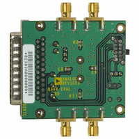
Manufacturer Part Number
AD8369-EVAL
Description
BOARD EVAL FOR AD8369
Manufacturer
Analog Devices Inc
Datasheet
1.AD8369-EVAL.pdf
(24 pages)
Specifications of AD8369-EVAL
Lead Free Status / RoHS Status
Contains lead / RoHS non-compliant


AD8369
Pin No. Mnemonic
10
11
12
13
14
15
16
1
2
3
4
5
6
7
8
9
INLO
COMM
BIT0
BIT1
BIT2
BIT3
DENB
OPLO
OPHI
CMDC
FILT
SENB
VPOS
PWUP
COMM
INHI
Function
Balanced Differential Input. Internally biased, should be ac-coupled.
Device Common. Connect to low impedance ground.
Gain Selection Least Significant Bit. Used as DATA input signal when in serial mode of operation.
Gain Selection Control Bit. Used as CLOCK input pin when in serial mode of operation.
Gain Selection Control Bit. Inactive when in serial mode of operation.
Gain Selection Most Significant Bit. Inactive when in serial mode of operation.
Data Enable Pin. Writes data to register. See Timing Specifications for details.
Balanced Differential Output. Biased to midsupply, should be ac-coupled.
Balanced Differential Output. Biased to midsupply, should be ac-coupled.
Common-Mode Decoupling Pin. Connect bypass capacitor to ground for additional common-mode supply
decoupling beyond the existing internal decoupling.
High-Pass Filter Connection. Used to set high-pass corner frequency.
Serial or Parallel Interface Select. Connect SENB to VPOS for serial operation. Connect SENB to COMM
for parallel operation.
Positive Supply Voltage, V
Power-Up Pin. Connect PWUP to VPOS to power up the device. Connect PWUP to COMM to power-down.
Device Common. Connect to a low impedance ground.
Balanced Differential Input. Internally biased, should be ac-coupled.
PIN FUNCTION DESCRIPTIONS
COMM
DENB
OPLO
INLO
BIT0
BIT1
BIT2
BIT3
S
PIN CONFIGURATION
= +3 V to +5.5 V.
1
6
7
8
2
3
4
5
(Not To Scale)
AD8369
TOP VIEW
–6–
16
15
14
13
12
11
10
9
INHI
COMM
PWUP
VPOS
SENB
FILT
CMDC
OPHI
REV. 0
Related parts for AD8369-EVAL
Image
Part Number
Description
Manufacturer
Datasheet
Request
R

Part Number:
Description:
BOARD EVAL FOR AD8369 LF-600MHZ
Manufacturer:
Analog Devices Inc

Part Number:
Description:
±1.7g Dual-Axis IMEMS Accelerometer Evaluation Board
Manufacturer:
Analog Devices Inc
Datasheet:
Part Number:
Description:
Inertial Sensor Evaluation System
Manufacturer:
Analog Devices Inc
Datasheet:
Part Number:
Description:
Manufacturer:
Analog Devices Inc
Datasheet:
Part Number:
Description:
Manufacturer:
Analog Devices Inc
Datasheet:
Part Number:
Description:
Manufacturer:
Analog Devices Inc
Datasheet:
Part Number:
Description:
Manufacturer:
Analog Devices Inc
Datasheet:
Part Number:
Description:
Manufacturer:
Analog Devices Inc
Datasheet:
Part Number:
Description:
Manufacturer:
Analog Devices Inc
Datasheet:
Part Number:
Description:
Manufacturer:
Analog Devices Inc
Datasheet:
Part Number:
Description:
Manufacturer:
Analog Devices Inc
Datasheet:
Part Number:
Description:
Manufacturer:
Analog Devices Inc
Datasheet:
Part Number:
Description:
Manufacturer:
Analog Devices Inc
Datasheet: