AD8330-EVAL Analog Devices Inc, AD8330-EVAL Datasheet - Page 29
AD8330-EVAL
Manufacturer Part Number
AD8330-EVAL
Description
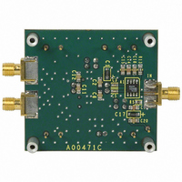
BOARD EVAL FOR AD8330
Manufacturer
Analog Devices Inc
Specifications of AD8330-EVAL
Rohs Status
RoHS non-compliant


OPTIONS
Table 6 lists the jumpers on the board and their functions.
Table 6. Functions of Jumpers
Name
FLTR
OFST
UP
DOWN
Connects a high-pass filter to the offset control loop
pin. This jumper is normally not installed.
Disables the offset correction loop. This jumper is
installed for dc or low frequency operation.
Mode up. Install for ascending gain with increasing
VDBS gain control voltage.
Mode down. Install for descending gain with
increasing VDBS gain control voltage.
Function
POWER SUPPLY
PRECISION VOLTAGE REFERENCES
+5V
(FOR VDBS, VMAG)
GND
SIGNAL
INPUT
Figure 71. Typical Connections
NETWORK
ANALYZER
Rev. E | Page 29 of 32
MEASUREMENT SETUP
The basic board connections for a typical measurement are
shown in Figure 71. To minimize circuit-loading effects, a low
capacitance FET probe is recommended for observing input or
output waveforms. Two-pin headers, IN_TEST and OUT_TEST,
are provided for this purpose. The SMA connectors OUT_HI
and OUT_LO can also be used, but the user may need to
account for load capacitance effects.
AD8330-EVALZ BOARD DESIGN
The AD8330-EVALZ is a 4-layer design for maximum ground-
plane area. The evaluation board side silkscreen and wiring
patterns are shown in Figure 72 through Figure 77.
POWER SUPPLY
DIFFERENTIAL
PROBE
PROBE
AD8330
Related parts for AD8330-EVAL
Image
Part Number
Description
Manufacturer
Datasheet
Request
R

Part Number:
Description:
BOARD EVAL FOR AD8330
Manufacturer:
Analog Devices Inc
Datasheet:

Part Number:
Description:
±1.7g Dual-Axis IMEMS Accelerometer Evaluation Board
Manufacturer:
Analog Devices Inc
Datasheet:

Part Number:
Description:
Inertial Sensor Evaluation System
Manufacturer:
Analog Devices Inc
Datasheet:
Part Number:
Description:
Manufacturer:
Analog Devices Inc
Datasheet:
Part Number:
Description:
Manufacturer:
Analog Devices Inc
Datasheet:
Part Number:
Description:
Manufacturer:
Analog Devices Inc
Datasheet:
Part Number:
Description:
Manufacturer:
Analog Devices Inc
Datasheet:
Part Number:
Description:
Manufacturer:
Analog Devices Inc
Datasheet:
Part Number:
Description:
Manufacturer:
Analog Devices Inc
Datasheet:
Part Number:
Description:
Manufacturer:
Analog Devices Inc
Datasheet:
Part Number:
Description:
Manufacturer:
Analog Devices Inc
Datasheet:
Part Number:
Description:
Manufacturer:
Analog Devices Inc
Datasheet:
Part Number:
Description:
Manufacturer:
Analog Devices Inc
Datasheet: