NLSF595EVB ON Semiconductor, NLSF595EVB Datasheet - Page 4
NLSF595EVB
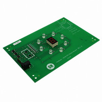
Manufacturer Part Number
NLSF595EVB
Description
BOARD EVAL TRICOLOR LED DRIVER
Manufacturer
ON Semiconductor
Specifications of NLSF595EVB
Design Resources
NLSF595 Demo Board BOM NLSF595EVB Gerber Files
Lead Free Status / RoHS Status
Contains lead / RoHS non-compliant
For Use With/related Products
NLSF595
Other names
NLSF595EVB
NLSF595EVBOS
NLSF595EVBOS


Maximum ratings are those values beyond which device damage can occur. Maximum ratings applied to the device are individual stress limit
values (not normal operating conditions) and are not valid simultaneously. If these limits are exceeded, device functional operation is not implied,
damage may occur and reliability may be affected.
1. Tested to EIA/JESD78
SR = shift register contents
STR = storage register contents
MAXIMUM RATINGS
Transfer shift register
contents to storage
register
RECOMMENDED OPERATING CONDITIONS
FUNCTION TABLE
Clear shift register
Shift data into shift
register
Registers remains
unchanged
Storage register remains
unchanged
Enable parallel outputs
Force outputs into high
impedance state
I
Symbol
LATCHUP
Symbol
V
T
V
I
V
V
V
I
OUT
I
q
P
V
t
STG
OUT
I
OK
CC
OUT
T
r
CC
IK
JA
, t
CC
IN
D
IN
A
f
Operation
DC Supply Voltage
DC Input Voltage
DC Output Voltage
Operating Temperature Range, all Package Types
Input Rise or Fall Time
Positive DC Supply Voltage
Digital Input Voltage
DC Output Voltage
Input Diode Current
Output Diode Current
DC Output Current, per Pin
DC Supply Current, V
Power Dissipation in Still Air
Storage Temperature Range
Latchup Performance
Thermal Resistance, Junction−to−Ambient
(SCLR)
Reset
H
H
H
X
X
X
L
CC
D = data (L, H) logic level
U = remains unchanged
Serial
and GND Pins
Input
(SI)
D
X
X
X
X
X
X
Characteristics
L, H, ↓
L, H, ↓
Inputs
(SCK)
Clock
Shift
X
↑
X
X
X
Parameter
http://onsemi.com
Above V
L, H, ↓
L, H, ↓
L, H, ↓
Clock
(RCK)
Reg
X
X
X
↑
NLSF595
CC
↓ = High−to−Low
↑ = Low−to−High
4
Output
Enable
and Below GND at 125°C (Note 1)
(OE)
H
L
L
L
L
L
L
V
V
CC
CC
SR
Contents
= 3.3 V + 0.3 V
= 5.0 V + 0.5 V
Register
D→SR
N
Shift
→SR
U
U
L
*
*
*
A
N+1
* = depends on Reset and Shift Clock inputs
** = depends on Register Clock input
;
SR
Contents
Resulting Function
Register
Storage
N
³STR
U
U
**
U
**
**
Min
−55
2.0
0
0
0
N
−0.5 to V
−0.5 to +7.0
−0.5 to +7.0
−65 to +150
SR
Output
(SQH)
Value
$300
Serial
$50
$75
G
−20
+50
450
128
Max
V
125
5.5
5.5
50
15
→SR
U
L
CC
*
*
*
*
CC
+7.0
H
(QA − QH)
Outputs
Enabled
Parallel
Unit
ns/V
SR
°C
**
V
V
V
U
U
U
Z
°C/W
Unit
mW
N
mA
mA
mA
mA
mA
°C
V
V
V
Related parts for NLSF595EVB
Image
Part Number
Description
Manufacturer
Datasheet
Request
R

Part Number:
Description:
Tri-color Led Driver
Manufacturer:
ON Semiconductor
Datasheet:

Part Number:
Description:
Buffers & Line Drivers 2-5.5V Quad Bus
Manufacturer:
ON Semiconductor
Datasheet:
Part Number:
Description:
ON Semiconductor [VOLTAGE REGULATOR]
Manufacturer:
ON Semiconductor
Datasheet:
Part Number:
Description:
357-036-542-201 CARDEDGE 36POS DL .156 BLK LOPRO
Manufacturer:
ON Semiconductor
Datasheet:
Part Number:
Description:
357-036-542-201 CARDEDGE 36POS DL .156 BLK LOPRO
Manufacturer:
ON Semiconductor
Datasheet:
Part Number:
Description:
357-036-542-201 CARDEDGE 36POS DL .156 BLK LOPRO
Manufacturer:
ON Semiconductor
Datasheet:
Part Number:
Description:
357-036-542-201 CARDEDGE 36POS DL .156 BLK LOPRO
Manufacturer:
ON Semiconductor
Datasheet:
Part Number:
Description:
357-036-542-201 CARDEDGE 36POS DL .156 BLK LOPRO
Manufacturer:
ON Semiconductor
Datasheet:
Part Number:
Description:
357-036-542-201 CARDEDGE 36POS DL .156 BLK LOPRO
Manufacturer:
ON Semiconductor
Datasheet:
Part Number:
Description:
357-036-542-201 CARDEDGE 36POS DL .156 BLK LOPRO
Manufacturer:
ON Semiconductor
Datasheet:
Part Number:
Description:
357-036-542-201 CARDEDGE 36POS DL .156 BLK LOPRO
Manufacturer:
ON Semiconductor
Datasheet:
Part Number:
Description:
357-036-542-201 CARDEDGE 36POS DL .156 BLK LOPRO
Manufacturer:
ON Semiconductor
Datasheet:
Part Number:
Description:
357-036-542-201 CARDEDGE 36POS DL .156 BLK LOPRO
Manufacturer:
ON Semiconductor
Datasheet:
Part Number:
Description:
Manufacturer:
ON Semiconductor
Datasheet: