NBSG11BAEVB ON Semiconductor, NBSG11BAEVB Datasheet - Page 3
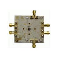
NBSG11BAEVB
Manufacturer Part Number
NBSG11BAEVB
Description
BOARD EVALUATION BBG NBSG11BA
Manufacturer
ON Semiconductor
Specifications of NBSG11BAEVB
Technology Type
Evaluation Board
Lead Free Status / RoHS Status
Contains lead / RoHS non-compliant
For Use With/related Products
NBSG11
Other names
NBSG11BAEVB
NBSG11BAEVBOS
NBSG11BAEVBOS


Setup (continued)
Step 3:
Step 4:
Amplitude = 500 mV
Offset = 660 mV
Advantest D3186
Signal Generator
(12 GHz)
NOTE:
NOTE:
TRIGGER
NOTE:
NOTE:
Setup Input Signals
Connect Output Signals
3a: Set the signal generator amplitude to 500 mV.
3b: Set the signal generator offset to 660 mV (the center of a nominal RSECL output).
3c: Set the generator output for a PRBS data signal, or for a square wave clock signal with
a 50% duty cycle.
4a: Connect the outputs of the device (Q0, Q1,
sampling head must have internal 50 W termination to ground.
All differential cable pairs must be matched.
OUT
OUT
Where a single output is being used, the unconnected output for the pair must be terminated to
V
V
The signal generator amplitude can vary from 75 mV to 900 mV to produce a 400 mV DUT
output.
The V
vary as long as V
information.
TT
TT
through a 50 W resistor for best operation. Unused pairs may be left unconnected. Since
= 0 V, a standard 50 W SMA termination is recommended.
GND
AC Coupling
IHCMR
50
(Input High Voltage Common Mode Range) allows the signal generator offset to
W
Figure 3. NBSG11 Board Setup - Time Domain
IH
is within the V
CLK
CLK
V
EE
= -1.3 V (3.3 V op)
(Single-Ended Mode)
V
V
V
NBSG11BAEVB
http://onsemi.com
CC
CC
EE
IHCMR
= 2.0 V
range. Refer to the device data sheet for further
3
Q1
Q0
) to the oscilloscope. The oscilloscope
V
V
TT
TT
Q0
Q1
GND
GND
= 0 V
= 0 V
Channel 1 (80E01)
Channel 2 (80E01)
Channel 3 (80E01)
Channel 4 (80E01)
TRIGGER
Tektronix TDS8000
Digital Oscilloscope
Related parts for NBSG11BAEVB
Image
Part Number
Description
Manufacturer
Datasheet
Request
R

Part Number:
Description:
Buffers & Line Drivers 2.5V/3.3V Multilevel
Manufacturer:
ON Semiconductor

Part Number:
Description:
ON Semiconductor [VOLTAGE REGULATOR]
Manufacturer:
ON Semiconductor
Datasheet:
Part Number:
Description:
357-036-542-201 CARDEDGE 36POS DL .156 BLK LOPRO
Manufacturer:
ON Semiconductor
Datasheet:
Part Number:
Description:
357-036-542-201 CARDEDGE 36POS DL .156 BLK LOPRO
Manufacturer:
ON Semiconductor
Datasheet:
Part Number:
Description:
357-036-542-201 CARDEDGE 36POS DL .156 BLK LOPRO
Manufacturer:
ON Semiconductor
Datasheet:
Part Number:
Description:
357-036-542-201 CARDEDGE 36POS DL .156 BLK LOPRO
Manufacturer:
ON Semiconductor
Datasheet:
Part Number:
Description:
357-036-542-201 CARDEDGE 36POS DL .156 BLK LOPRO
Manufacturer:
ON Semiconductor
Datasheet:
Part Number:
Description:
357-036-542-201 CARDEDGE 36POS DL .156 BLK LOPRO
Manufacturer:
ON Semiconductor
Datasheet:
Part Number:
Description:
357-036-542-201 CARDEDGE 36POS DL .156 BLK LOPRO
Manufacturer:
ON Semiconductor
Datasheet:
Part Number:
Description:
357-036-542-201 CARDEDGE 36POS DL .156 BLK LOPRO
Manufacturer:
ON Semiconductor
Datasheet:
Part Number:
Description:
357-036-542-201 CARDEDGE 36POS DL .156 BLK LOPRO
Manufacturer:
ON Semiconductor
Datasheet:
Part Number:
Description:
357-036-542-201 CARDEDGE 36POS DL .156 BLK LOPRO
Manufacturer:
ON Semiconductor
Datasheet:
Part Number:
Description:
Manufacturer:
ON Semiconductor
Datasheet: