NBSG11BAEVB ON Semiconductor, NBSG11BAEVB Datasheet
NBSG11BAEVB
Specifications of NBSG11BAEVB
NBSG11BAEVBOS


Related parts for NBSG11BAEVB


NBSG11BAEVB Summary of contents
Page 1
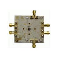
... Eye Pattern Generation Frequency Performance Output Rise and Fall Time V (Input High Common Mode Range) IHCMR 1. Single- ended measurements can only be made 3.3 V using this board setup Figure 1. NBSG11 Evaluation Board 1 http://onsemi.com EVALUATION BOARD MANUAL (1) or differential modes Publication Order Number: NBSG11BAEVB/D ...
Page 2
... OUT Amplitude = 500 mV Offset = 660 mV TRIGGER NOTE: All differential cable pairs must be matched. Figure 2. NBSG11 Board Setup - Time Domain NBSG11BAEVB Setup for Time Domain Measurements Example Equipment (Note 1) HP6624A TDS8000 with 80E01 Sampling Head (Note 2) HP 8133A, Advantest D3186 Storm, Semflex ...
Page 3
... GHz) AC Coupling OUT OUT Amplitude = 500 mV Offset = 660 GND TRIGGER NOTE: All differential cable pairs must be matched. Figure 3. NBSG11 Board Setup - Time Domain NBSG11BAEVB is within the V range. Refer to the device data sheet for further IH IHCMR ) to the oscilloscope. The oscilloscope GND ...
Page 4
... NOTE: For frequency domain measurements, 2.5 V power supply is not recommended because additional equipment (bias tee, etc.) is needed for proper operation. The input signal has to be properly offset to meet V NBSG11BAEVB Example Equipment (Note 3) HP 6624A R&S ZVK (10MHz to 40 GHz) Krytar Model #4010180 ...
Page 5
... Step 3: 3a: Set display to measure S21 and record data. PORT 1 GND 50 W Hybrid Coupler NOTE: Hybrid Coupler has equal power split (3dB) with 180 between outputs Figure 4. NBSG11 Board Setup – Frequency Domain NBSG11BAEVB Rohde & Schwartz Vector Network Analyzer GND ...
Page 6
... Set input levels to +2.0 dBm (500 mV) at the input of DUT. Output Setup Step 3: 3a: Set display to measure S21 and record data. PORT GND NOTE: Unused Input “DC Blocked” Figure 5. NBSG11 Board Setup – Frequency Domain NBSG11BAEVB Rohde & Schwartz Vector Network Analyzer GND ...
Page 7
... ROSENBERGER SMA T1 1 ROSENBERGER SMA Decoupling cap and Transmission line NOTE: NBSG11BAEVB The following considerations played a key role to ensure this evaluation board achieves high-end microwave performance: Optimal SMA connector launch Minimal insertion loss and signal dispersion Accurate Transmission line matching (50 ohms) ...
Page 8
... Dielectric (5.0 mil) Thick Copper Base Figure 7. Board Stack- START 1 GHz NOTE: The insertion loss curve can be used to calibrate out board loss if testing under small signal conditions. NBSG11BAEVB Description Manufacturer ON Semiconductor Rosenberger Dielectric Laboratories 5.0 mil 32 mil PIN 1 Figure 8. Layout Mask for NBSG11 1 GHz/ Figure 9 ...
Page 9
... FREQUENCY (GHz) Figure 10. Fmax - Amplitude vs. Frequency (NBSG11 3 255C Input Amplitude 500 mV -40 Figure 12. NBSG11 T Figure 13. NBSG11: Eye Diagram at 10 Gbps with PRBS 2^31-1 (total system jitter including signal generator is shown) NBSG11BAEVB -40 -20 Figure 11. NBSG11 T 3.3 V 2 TEMPERATURE ( C) vs. Temperature and Supply Voltage f http://onsemi ...
Page 10
... START 10 MHz 1 GHz/ Figure 14. NBSG11: Small Signal Gain (S21 Q1B 10 dB -40 dB START 10 MHz 1 GHz/ Figure 16. NBSG11 Return Loss (S11) Q0 – Q1B NBSG11BAEVB CC 11 GHz 25 dB -25 dB STOP 12 GHz START 1 GHz Figure 15. NBSG11: Large Signal Gain (S21) 11 GHz 10 dB -40 dB ...
Page 11
... IBIS and Spice models ORDERING INFORMATION Orderable Part No NBSG11BA Differential Receiver/Driver with RSECL Outputs NBSG11BAR2 Differential Receiver/Driver with RSECL Outputs NBSG11BAEVB NBSG11 Evaluation Board NBSG11BAEVB References NBSG11/D, Data Receiver/Driver with RSECL Outputs. AND8077/D, Application Note, GigaCommt (SiGe) SPICE Modeling Kit. AND8075/D, Application Considerations for the FCBGA Packages ...
Page 12
... DATUM Z (SEATING PLANE) IS DEFINED BY THE SPHERICAL CROWNS OF THE SOLDER BALLS. 5. PARALLELISM MEASUREMENT SHALL EXCLUDE ANY EFFECT OF MARK ON TOP SURFACE OF PACKAGE. MILLIMETERS DIM MIN MAX A 1.40 MAX A1 0.25 0.35 A2 1.20 REF b 0.30 0.50 D 4.00 BSC E 4.00 BSC e 1.00 BSC S 0.50 BSC NBSG11BAEVB/D ...