AT18F-DK3 Atmel, AT18F-DK3 Datasheet - Page 13
AT18F-DK3
Manufacturer Part Number
AT18F-DK3
Description
KIT CONFIG PROGRAM FOR AT18F FAM
Manufacturer
Atmel
Series
AT18Fr
Type
In-Circuit Emulator Systemr
Datasheet
1.ATF15XXDK3-SAX20.pdf
(22 pages)
Specifications of AT18F-DK3
Contents
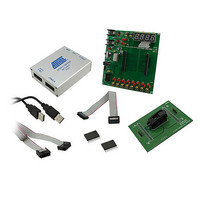
2 Boards, Cable, CD, Samples
Processor To Be Evaluated
AT18F
Processor Series
AT18F
Interface Type
ISP, JTAG
Operating Supply Voltage
3.3 V
For Use With/related Products
AT18F Series
Lead Free Status / RoHS Status
Lead free / RoHS Compliant
Other names
Q4623814


3685A–CNFG–04/08
Hardware Description
2-8
The ISP algorithm is controlled by the JCPS (JTAG Configurator Programming System) software, which
is running on the PC. The four JTAG signals are generated by the LPT port and they are buffered by the
ISP download cable before going into the ATF15xx-DK3 Base Board of the AT18F-DK3 kit. The pinout
for the 10-pin JTAG Port Header on the ATF15xx-DK3 Base Board is shown in
dimensions of this 10-pin male JTAG header are shown in
Figure 2-8.
Figure 2-9.
Notes:
1. All dimensions are in inches.
2. Pitch = 1-inch = 2.54 mm
Pinout Diagram of 10-pin JTAG Port Header (Top-view)
10-pin Male Header Dimensions
Top View
GND
GND
VCC
0.100
NC
NC
10
8
6
4
2
AT18F-DK3 Configurator Development Kit User Guide
0.100
9
7
5
3
1
Side View
Figure
TDI
NC
TMS
TDO
TCK
0.025 Sq.
2-9.
0.235
Figure 2-8
and the
Related parts for AT18F-DK3
Image
Part Number
Description
Manufacturer
Datasheet
Request
R

Part Number:
Description:
ACCY USB CABLE JTAG ISP AT18F
Manufacturer:
Atmel
Datasheet:

Part Number:
Description:
DEV KIT FOR AVR/AVR32
Manufacturer:
Atmel
Datasheet:

Part Number:
Description:
INTERVAL AND WIPE/WASH WIPER CONTROL IC WITH DELAY
Manufacturer:
ATMEL Corporation
Datasheet:
Part Number:
Description:
Low-Voltage Voice-Switched IC for Hands-Free Operation
Manufacturer:
ATMEL Corporation
Datasheet:
Part Number:
Description:
MONOLITHIC INTEGRATED FEATUREPHONE CIRCUIT
Manufacturer:
ATMEL Corporation
Datasheet:
Part Number:
Description:
AM-FM Receiver IC U4255BM-M
Manufacturer:
ATMEL Corporation
Datasheet:
Part Number:
Description:
Monolithic Integrated Feature Phone Circuit
Manufacturer:
ATMEL Corporation
Datasheet:
Part Number:
Description:
Multistandard Video-IF and Quasi Parallel Sound Processing
Manufacturer:
ATMEL Corporation
Datasheet:
Part Number:
Description:
High-performance EE PLD
Manufacturer:
ATMEL Corporation
Datasheet:
Part Number:
Description:
8-bit Flash Microcontroller
Manufacturer:
ATMEL Corporation
Datasheet:
Part Number:
Description:
2-Wire Serial EEPROM
Manufacturer:
ATMEL Corporation
Datasheet: