DEMO9S12NE64E Freescale Semiconductor, DEMO9S12NE64E Datasheet - Page 14
DEMO9S12NE64E
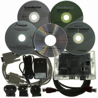
Manufacturer Part Number
DEMO9S12NE64E
Description
DEMO BOARD FOR 9S12NE64
Manufacturer
Freescale Semiconductor
Type
MCUr
Datasheet
1.DEMO9S12NE64E.pdf
(21 pages)
Specifications of DEMO9S12NE64E
Contents
*
Processor To Be Evaluated
MC9S12NE64
Maximum Operating Temperature
+ 50 C
Minimum Operating Temperature
- 10 C
Operating Supply Voltage
6 V to 12 V
Silicon Manufacturer
Freescale
Core Architecture
S12
Core Sub-architecture
S12
Silicon Core Number
MC9S12
Silicon Family Name
S12NE
Rohs Compliant
Yes
For Use With/related Products
MC9S12NE64
Lead Free Status / RoHS Status
Lead free / RoHS Compliant


Freescale Semiconductor
10, 12, 14, 16,
18, 20, 22, 24
13, 15, 34, 36
Pin
11
17
19
21
23
25
26
27
28
29
30
31
32
33
35
37
38
Table 2-2 I/O Connector (J50) Signal Descriptions (Continued)
PT<4>, PT<5>,
PT<6>, PT<7>
PAD<0> -
PAD<7>
PH<5>
PG<0>
PG<1>
PG<2>
PG<3>
PG<4>
PG<5>
PG<6>
PS<5>
PS<4>
PS<6>
PS<7>
PS<2>
PJ<6>
PJ<7>
PJ<2>
PJ<3>
Label
DEMO9S12NE64 User’s Manual, Rev. 0.8
PAD[7:0] are the analog inputs for the analog to digital converter (ADC). They
can also be configured as general purpose digital input
PH5 is a general purpose input or output pin. When the EMAC MII interface is
enabled it becomes the transmit Enabled (MII_TXEN) signal
PT[7:4] are general purpose input or output pins. When the Timer system 1
(TIM1) is enabled they can also be configured as the TIM1 input capture or
output compare pins IOC1[7-4]
PS5 is a general purpose input or output pin. When the Serial Peripheral
Interface (SPI) is enabled PS5 is the master output (during master mode) or
slave input (during slave mode) pin (MOSI)
PS4 is a general purpose input or output pin. When the Serial Peripheral
Interface (SPI) is enabled PS4 is the master input (during master mode) or
slave output (during slave mode) pin (MISO)
PS6 is a general purpose input or output pin. When the Serial Peripheral
Interface (SPI) is enabled PS6 becomes the serial clock pin, SCK
PS7 is a general purpose input or output. When the Serial Peripheral Interface
(SPI) is enabled PS7 becomes the slave select pin SS
PG6 is a general purpose input or output pin. When the EMAC MII interface is
enabled it becomes the receive data (MII_RXD0) signal
PJ6 is a general purpose input or output pin. When the IIC module is enabled it
becomes the Serial Data Line (IIC_SDL) for the IIC module (IIC)
PG1 is a general purpose input or output pin. When the EMAC MII interface is
enabled it becomes the receive data (MII_RXD1) signal
PJ7 is a general purpose input or output pin. When the IIC module is enabled it
becomes the serial clock line (IIC_SCL) for the IIC module (IIC)
PG2 is a general purpose input or output pin. When the EMAC MII interface is
enabled it becomes the receive data (MII_RXD2) signal
PJ2 is a general purpose input or output pin. When the EMAC MII interface is
enabled it becomes the carrier sense (MII_CRS) signal
PG3 is a general purpose input or output pin. When the EMAC MII interface is
enabled it becomes the receive data (MII_RXD3) signal
PJ3 is a general purpose input or output pin. When the EMAC MII interface is
enabled it becomes the collision (MII_COL) signal
PG4 is a general purpose input or output pin. When the EMAC MII interface is
enabled it becomes the receive clock (MII_RXCLK) signal
PG5 is a general purpose input or output pin. When the EMAC MII interface is
enabled it becomes the receive data valid (MII_RXDV) signal
PG6 is a general purpose input or output pin. When the EMAC MII interface is
enabled it becomes the receive error (MII_RXER) signal
PS2 is a general purpose input or output. When the Serial Communications
Interface 1 (SCI1) receiver is enabled the PS2 pin is configured as the receive
pin RXD of SCI1
Signal
Support Information
17
Related parts for DEMO9S12NE64E
Image
Part Number
Description
Manufacturer
Datasheet
Request
R

Part Number:
Description:
Manufacturer:
Freescale Semiconductor, Inc
Datasheet:
Part Number:
Description:
Manufacturer:
Freescale Semiconductor, Inc
Datasheet:
Part Number:
Description:
Manufacturer:
Freescale Semiconductor, Inc
Datasheet:
Part Number:
Description:
Manufacturer:
Freescale Semiconductor, Inc
Datasheet:
Part Number:
Description:
Manufacturer:
Freescale Semiconductor, Inc
Datasheet:
Part Number:
Description:
Manufacturer:
Freescale Semiconductor, Inc
Datasheet:
Part Number:
Description:
Manufacturer:
Freescale Semiconductor, Inc
Datasheet:
Part Number:
Description:
Manufacturer:
Freescale Semiconductor, Inc
Datasheet:
Part Number:
Description:
Manufacturer:
Freescale Semiconductor, Inc
Datasheet:
Part Number:
Description:
Manufacturer:
Freescale Semiconductor, Inc
Datasheet:
Part Number:
Description:
Manufacturer:
Freescale Semiconductor, Inc
Datasheet:
Part Number:
Description:
Manufacturer:
Freescale Semiconductor, Inc
Datasheet:
Part Number:
Description:
Manufacturer:
Freescale Semiconductor, Inc
Datasheet:
Part Number:
Description:
Manufacturer:
Freescale Semiconductor, Inc
Datasheet:
Part Number:
Description:
Manufacturer:
Freescale Semiconductor, Inc
Datasheet: