DEMO9RS08LA8 Freescale Semiconductor, DEMO9RS08LA8 Datasheet - Page 8
DEMO9RS08LA8
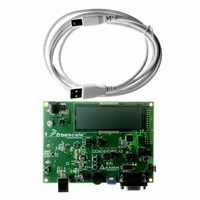
Manufacturer Part Number
DEMO9RS08LA8
Description
BOARD DEMO FOR MC9RSOLA8 MCU
Manufacturer
Freescale Semiconductor
Series
RS08r
Type
MCUr
Datasheets
1.DEMO9RS08LA8.pdf
(14 pages)
2.DEMO9RS08LA8.pdf
(8 pages)
3.DEMO9RS08LA8.pdf
(34 pages)
4.DEMO9RS08LA8.pdf
(2 pages)
Specifications of DEMO9RS08LA8
Contents
Board, Cable, DVD
Silicon Manufacturer
Freescale
Core Architecture
RS08
Core Sub-architecture
RS08
Silicon Core Number
MC9RS08
Silicon Family Name
RS08LA
Kit Contents
Board Cables CD Docs
Rohs Compliant
Yes
For Use With/related Products
MC9RS08LA8
Lead Free Status / RoHS Status
Contains lead / RoHS non-compliant
Available stocks
Company
Part Number
Manufacturer
Quantity
Price
Company:

Part Number:
DEMO9RS08LA8
Manufacturer:
Freescale Semiconductor
Quantity:
135


Electrical Characteristics
3.3
This section provides information about operating temperature range, power dissipation, and package
thermal resistance. Power dissipation on I/O pins is usually small compared to the power dissipation in
on-chip logic and voltage regulator circuits and it is user-determined rather than being controlled by the
MCU design. In order to take P
actual pin voltage and V
unusually high pin current (heavy loads), the difference between pin voltage and V
small.
The average chip-junction temperature (TJ) in °C can be obtained from:
where:
T
θ
P
P
P
For most applications, P
8
JA
A
D
int
I/O
= Ambient temperature, °C
1
2
3
= P
= Package thermal resistance, junction-to-ambient, °C /W
= I
= Power dissipation on input and output pins user determined
Input must be current limited to the value specified. To determine the value of the required current-limiting resistor,
calculate resistance values for positive (V
resistance values.
All functional non-supply pins are internally clamped to V
clamped to V
Power supply must maintain regulation within operating V
current conditions. If positive injection current (V
and could result in external power supply going out of regulation. Ensure external V
than maximum injection current. This will be the greatest risk when the MCU is not consuming power. Examples are:
if no system clock is present, or if the clock rate is very low which would reduce overall power consumption.
int
DD
Operating temperature range (packaged)
Maximum junction temperature
Thermal resistance
Single layer board
Four layer board
+ P
Thermal Characteristics
× V
I/O
DD
SS
, Watts chip internal power
only.
I/O
SS
Rating
or V
<< P
I/O
DD
int
MC9RS08LA8 Series MCU Data Sheet, Rev. 1
into account in power calculations, determine the difference between
and can be neglected. An approximate relationship between PD and TJ
and multiply by the pin current for each I/O pin. Except in cases of
Table 4. Thermal Characteristics
48-pin LQFP
48-pin LQFP
DD
48-pin QFN
48-pin QFN
T
J
) and negative (V
= T
In
A
> V
+ (P
DD
T
T
θ
D
) is greater than I
A
JA
JMAX
SS
DD
× θ
Symbol
and V
range during instantaneous and operating maximum
JA
SS
)
) clamp voltages, then use the larger of the two
DD
except the RESET/V
T
–40 to 85
105
71
84
49
28
L
DD
to T
, the injection current may flow out of V
H
Value
DD
load will shunt current greater
PP
pin which is internally
SS
Freescale Semiconductor
or V
°C
°C
°C/W
DD
Unit
will be very
Eqn. 1
DD
Related parts for DEMO9RS08LA8
Image
Part Number
Description
Manufacturer
Datasheet
Request
R

Part Number:
Description:
Manufacturer:
Freescale Semiconductor, Inc
Datasheet:
Part Number:
Description:
Manufacturer:
Freescale Semiconductor, Inc
Datasheet:
Part Number:
Description:
Manufacturer:
Freescale Semiconductor, Inc
Datasheet:
Part Number:
Description:
Manufacturer:
Freescale Semiconductor, Inc
Datasheet:
Part Number:
Description:
Manufacturer:
Freescale Semiconductor, Inc
Datasheet:
Part Number:
Description:
Manufacturer:
Freescale Semiconductor, Inc
Datasheet:
Part Number:
Description:
Manufacturer:
Freescale Semiconductor, Inc
Datasheet:
Part Number:
Description:
Manufacturer:
Freescale Semiconductor, Inc
Datasheet:
Part Number:
Description:
Manufacturer:
Freescale Semiconductor, Inc
Datasheet:
Part Number:
Description:
Manufacturer:
Freescale Semiconductor, Inc
Datasheet:
Part Number:
Description:
Manufacturer:
Freescale Semiconductor, Inc
Datasheet:
Part Number:
Description:
Manufacturer:
Freescale Semiconductor, Inc
Datasheet:
Part Number:
Description:
Manufacturer:
Freescale Semiconductor, Inc
Datasheet:
Part Number:
Description:
Manufacturer:
Freescale Semiconductor, Inc
Datasheet:
Part Number:
Description:
Manufacturer:
Freescale Semiconductor, Inc
Datasheet: