DEMO9RS08LA8 Freescale Semiconductor, DEMO9RS08LA8 Datasheet - Page 10
DEMO9RS08LA8
Manufacturer Part Number
DEMO9RS08LA8
Description
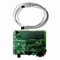
BOARD DEMO FOR MC9RSOLA8 MCU
Manufacturer
Freescale Semiconductor
Series
RS08r
Type
MCUr
Datasheets
1.DEMO9RS08LA8.pdf
(14 pages)
2.DEMO9RS08LA8.pdf
(8 pages)
3.DEMO9RS08LA8.pdf
(34 pages)
4.DEMO9RS08LA8.pdf
(2 pages)
Specifications of DEMO9RS08LA8
Contents
Board, Cable, DVD
Silicon Manufacturer
Freescale
Core Architecture
RS08
Core Sub-architecture
RS08
Silicon Core Number
MC9RS08
Silicon Family Name
RS08LA
Kit Contents
Board Cables CD Docs
Rohs Compliant
Yes
For Use With/related Products
MC9RS08LA8
Lead Free Status / RoHS Status
Contains lead / RoHS non-compliant
Available stocks
Company
Part Number
Manufacturer
Quantity
Price
Company:

Part Number:
DEMO9RS08LA8
Manufacturer:
Freescale Semiconductor
Quantity:
135


Electrical Characteristics
3.5
This section includes information about power supply requirements, I/O pin characteristics, and power
supply current in various operating modes.
10
Num
10
11
12
13
14
1
2
3
4
5
6
7
8
9
C
D
C
C
C
C
P
P
P
P
P
P
P
P
P
DC Characteristics
1
2
3
Supply voltage (run, wait and stop modes)
0 < f
Minimum RAM retention supply voltage applied to
V
Low-voltage Detection threshold
Power on RESET (POR) voltage
Input high voltage (V
Input high voltage (2.7 V ≤ V
inputs)
Input low voltage (V
Input low voltage (2.7 V ≤ V
(all digital inputs)
Input hysteresis (all digital inputs)
Input leakage current (per pin)
V
High impedance (off-state) leakage current (per pin)
V
Internal pullup/pulldown resistors
Output high voltage (all ports)
I
I
Maximum total I
OH
OH
DD
In
In
Parameter is achieved by design characterization on a small sample size from typical devices
under typical conditions unless otherwise noted.
These pins meet JESD78A Class II (section 1.2) Level A (section 1.3) requirement of ±100 mA.
This pin meets JESD78A Class II (section 1.2) Level B (section 1.3) characterization to ±75 mA.
= V
= V
= –5 mA (V
= –3 mA (V
No.
Bus
1
2
3
4
Table 7. DC Characteristics (Temperature Range = –40 to 85°C Ambient)
DD
DD
<10 MHz
or V
or V
Human body model (HBM)
Machine model (MM)
Charge device model (CDM)
Latch-up current at T
Latch-up current at T
SS ,
SS
DD ≥
DD ≥
OH
, all input/output
Table 6. ESD and Latch-Up Protection Characteristics
all input only pins
for all port pins
4.5 V)
3 V)
DD
Parameter
DD
> 5 V) (all digital inputs)
> 5V) (all digital inputs)
MC9RS08LA8 Series MCU Data Sheet, Rev. 1
Rating
DD
DD
3,4
≤ 5 V)
≤ 5 V) (all digital
2
(all port pins)
1
A
A
= 85°C
= 85°C
(V
DD
falling)
Symbol
V
V
V
I
I
Symbol
HBM
CDM
LAT
LAT
MM
V
|I
V
V
V
|I
V
R
V
V
V
|I
OHT
V
V
RAM
POR
LVD
OZ
hys
OH
DD
In
PU
IH
IH
IL
IL
|
|
|
0.70 × V
0.85 × V
0.06 × V
V
±2000
±100
±200
±500
±75
Min
DD –
0.8
Min
2.7
0.9
20
—
—
—
—
—
—
3
2
1
0.8
DD
DD
DD
Typical
0.025
0.025
Max
1.8
1.4
45
—
—
—
—
—
—
—
—
—
—
—
—
—
—
Freescale Semiconductor
0.30 × V
0.30 × V
Unit
mA
mA
Max
100
5.5
1.7
1.0
1.0
V
V
V
65
—
—
—
—
—
—
DD
DD
Unit
mA
μA
μA
kΩ
V
V
V
V
V
V
V
V
V
V
Related parts for DEMO9RS08LA8
Image
Part Number
Description
Manufacturer
Datasheet
Request
R

Part Number:
Description:
Manufacturer:
Freescale Semiconductor, Inc
Datasheet:
Part Number:
Description:
Manufacturer:
Freescale Semiconductor, Inc
Datasheet:
Part Number:
Description:
Manufacturer:
Freescale Semiconductor, Inc
Datasheet:
Part Number:
Description:
Manufacturer:
Freescale Semiconductor, Inc
Datasheet:
Part Number:
Description:
Manufacturer:
Freescale Semiconductor, Inc
Datasheet:
Part Number:
Description:
Manufacturer:
Freescale Semiconductor, Inc
Datasheet:
Part Number:
Description:
Manufacturer:
Freescale Semiconductor, Inc
Datasheet:
Part Number:
Description:
Manufacturer:
Freescale Semiconductor, Inc
Datasheet:
Part Number:
Description:
Manufacturer:
Freescale Semiconductor, Inc
Datasheet:
Part Number:
Description:
Manufacturer:
Freescale Semiconductor, Inc
Datasheet:
Part Number:
Description:
Manufacturer:
Freescale Semiconductor, Inc
Datasheet:
Part Number:
Description:
Manufacturer:
Freescale Semiconductor, Inc
Datasheet:
Part Number:
Description:
Manufacturer:
Freescale Semiconductor, Inc
Datasheet:
Part Number:
Description:
Manufacturer:
Freescale Semiconductor, Inc
Datasheet:
Part Number:
Description:
Manufacturer:
Freescale Semiconductor, Inc
Datasheet: