DV164039 Microchip Technology, DV164039 Datasheet - Page 39
DV164039
Manufacturer Part Number
DV164039
Description
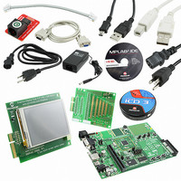
KIT DEV PIC24FJ256DA210
Manufacturer
Microchip Technology
Series
dsPIC™r
Type
MCUr
Specifications of DV164039
Contents
Dev Board, Display Board, 3 Bare Boards, MPLAB ICD-3, Cables, Power Supply
Processor To Be Evaluated
PIC24FJ256DA210
Data Bus Width
16 bit
Interface Type
RS-232, USB, Ethernet, SPI, UART
Operating Supply Voltage
9 V to 15 V
Silicon Manufacturer
Microchip
Core Architecture
PIC
Core Sub-architecture
PIC24
Silicon Core Number
PIC24F
Silicon Family Name
PIC24FJxxDAxxx
Lead Free Status / RoHS Status
Lead free / RoHS Compliant
For Use With/related Products
PIC24FJ256DA210
Lead Free Status / Rohs Status
Lead free / RoHS Compliant
Available stocks
Company
Part Number
Manufacturer
Quantity
Price
Company:

Part Number:
DV164039
Manufacturer:
MICROCHIP
Quantity:
12 000
Part Number:
DV164039
Manufacturer:
MICROCHIP/微芯
Quantity:
20 000


2010 Microchip Technology Inc.
4.4.2.3
To enable the USB OTG mode:
1. Install jumper J5.
2. Remove jumpers J6 and J7.
3. To detect the status of the regulated output voltage of the charge pump, connect
4. To have software control of the charge pump, connect the SHDN signal to the
In USB OTG mode, use J7 (Type Micro AB Female USB connector) to connect with
external USB OTG devices.
4.4.3
The development board provides one UART, with its RX and TX signals appearing on
pins RD0 and RF3 of the PIC24FJ256DA210, respectively. The signals can be
configured to appear at one of two places:
• The RS-232 external serial port (default).
• The PICtail Plus connector, as signals U1RX (pin 2) and U1TX (pin 4).
An RS-232 level shifter (U3) has been provided with all necessary hardware to support
the external serial port. The DB-9F serial connector (P1) is wired to support hardware
flow control; however, the flow control signals are not connected to the microcontroller.
The port is configured as a Data Communication Equipment (DCE) device.
The UART’s availability is configured by jumpers JP16 and JP17. Their location is
shown in Figure 4-5.
To access the UART through the RS-232 serial port:
1. Set jumper J16 to position 1-2 (USART_TX – TX) (default).
2. Set jumper J17 to position 1-2 (USART_RX – RX) (default).
In this configuration, a host PC running the appropriate application can communicate
with the development board using the serial channel. Use a standard
(“straight-through”) serial cable connected to P1.
To access the UART through the PICtail Plus expansion port:
1. Set jumper J16 to position 2-3 (U1TX – TX).
2. Set jumper J17 to position 2-3 (U1RX – RX).
In this configuration, the U1RX and U1TX signals appear at pins 2 and 4 of the PICtail
Plus connector, respectively.
Note:
Note:
the charge pump PGOOD signal to the microcontroller (Figure 4-4, callout 3):
a) Remove jumper JP14 (disconnects CTMU_PAD2, LED D2 and switch S2).
b) Populate resistor R32 with a
microcontroller (Figure 4-4, callout 3):
a) Remove jumper JP15 (disconnects the potentiometer, switch S3,
b) Populate resistor R45 with a
AN21/RE9).
CTMU_PAD3 and LED D3).
USB ON-THE-GO (OTG) MODE
UART (RS-232)
Enabling USB OTG mode may require the remapping of the UART’s TX
signal. See Section 4.4.3.1 “UART and USB OTG Mode (TX Remap-
ping)” for more information.
The TX and RX signals are mapped to the microcontroller pins using the
Peripheral Pin Select (PPS) feature. When developing applications, make
sure that the pins are remapped properly to use the UART Receive and
UART Transmit signals. Refer to Section 10.4 “Peripheral Pin Select” of
the PIC24FJ256DA210 data sheet for a detailed discussion of PPS.
Development Board Hardware
0
0
resistor (connects PGOOD signal to pin
resistor.
DS51911A-page 39
Related parts for DV164039
Image
Part Number
Description
Manufacturer
Datasheet
Request
R

Part Number:
Description:
Manufacturer:
Microchip Technology Inc.
Datasheet:
Part Number:
Description:
Manufacturer:
Microchip Technology Inc.
Datasheet:
Part Number:
Description:
Manufacturer:
Microchip Technology Inc.
Datasheet:
Part Number:
Description:
Manufacturer:
Microchip Technology Inc.
Datasheet:
Part Number:
Description:
Manufacturer:
Microchip Technology Inc.
Datasheet:
Part Number:
Description:
Manufacturer:
Microchip Technology Inc.
Datasheet:
Part Number:
Description:
Manufacturer:
Microchip Technology Inc.
Datasheet:
Part Number:
Description:
Manufacturer:
Microchip Technology Inc.
Datasheet: