C8051T606DK Silicon Laboratories Inc, C8051T606DK Datasheet - Page 9
C8051T606DK
Manufacturer Part Number
C8051T606DK
Description
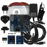
KIT DEVELOPMENT FOR C8051T606
Manufacturer
Silicon Laboratories Inc
Type
MCUr
Datasheets
1.C8051T600EDB.pdf
(188 pages)
2.C8051T606TDB.pdf
(1 pages)
3.C8051T606DK.pdf
(16 pages)
4.C8051T606TDB.pdf
(14 pages)
Specifications of C8051T606DK
Contents
Board, Adapter, Cable, CD, Power Supply
Processor To Be Evaluated
C8051T606x
Interface Type
RS-232, USB
Maximum Operating Temperature
+ 85 C
Minimum Operating Temperature
- 40 C
Operating Supply Voltage
3.3 V
Lead Free Status / RoHS Status
Lead free / RoHS Compliant
For Use With/related Products
C8051T606
Lead Free Status / Rohs Status
Lead free / RoHS Compliant
Other names
336-1666


7.7. VPP Connection (J10)
The C8051T60x devices require a special 6.5 V programming voltage applied to the VPP pin during device
programming. The VPP pin on these devices is shared with P0.2. During programming, the VPP voltage is
automatically enabled when needed. Header J10 is provided to allow the user to disconnect the programming
circuitry from the VPP/P0.2 pin to avoid interfering with the normal application operation of P0.2. When
programming the device, J10 should be shorted with a shorting block. When running normal application code, J10
can be removed. Note that the C8051T600 Emulation Daughter Board does not connect the main board’s VPP and
P0.2 signals, so removing the shorting block is not necessary when using the Emulation Daughter Board.
7.8. Using Alternate Supplies with the C8051T60x Development Kit
For most evaluation purposes, the on-board 3.3 V supply regulator is sufficient to be used as a VDD power supply.
However, in applications where a different supply voltage is desired (for example, 1.8 V), an external supply
voltage can be applied to the board at the analog connector (J6). Depending on the supply and the desired
functionality of the board, it may be necessary to cut the VDD supply voltage trace on the back of the board behind
header J9 (not populated). The following should be considered when supplying a different voltage to the device:
1. When programming a C8051T60x device: The on-board 3.3 V regulator should be used for VDD.
2. If a VDD supply voltage between 2.7 and 3.6 V is desired: The ac to dc power adapter should be disconnected
3. If a VDD supply voltage between 1.8 and 2.7 V is desired and RS-232 functionality is not required: The ac to dc
4. If a VDD supply voltage between 1.8 and 2.7 V is desired and RS-232 functionality is required: The RS-232
from P3, and the desired supply voltage can be applied directly to the GND and VDD terminals of terminal block
J6. No board modification is necessary.
power adapter should be disconnected from P3, and the desired supply voltage can be applied directly to the
GND and VDD terminals of terminal block J6. No board modification is necessary.
transceiver is not specified to operate below 2.7 V. In this case, the trace under header J9 should be cut. Then,
the desired VDD supply voltage can be applied directly to the GND and VDD terminals of terminal block J6, and
the ac to dc power adapter can be connected to P3, to provide 3.3 V to the RS-232 transceiver. In this case, it
may also be necessary to configure the TX pin on the device for open-drain mode, and add a pull-up resistor to
the supply of the transceiver.
Rev. 0.1
C8051T60x-DK
9
Related parts for C8051T606DK
Image
Part Number
Description
Manufacturer
Datasheet
Request
R

Part Number:
Description:
SMD/C°/SINGLE-ENDED OUTPUT SILICON OSCILLATOR
Manufacturer:
Silicon Laboratories Inc
Part Number:
Description:
Manufacturer:
Silicon Laboratories Inc
Datasheet:
Part Number:
Description:
N/A N/A/SI4010 AES KEYFOB DEMO WITH LCD RX
Manufacturer:
Silicon Laboratories Inc
Datasheet:
Part Number:
Description:
N/A N/A/SI4010 SIMPLIFIED KEY FOB DEMO WITH LED RX
Manufacturer:
Silicon Laboratories Inc
Datasheet:
Part Number:
Description:
N/A/-40 TO 85 OC/EZLINK MODULE; F930/4432 HIGH BAND (REV E/B1)
Manufacturer:
Silicon Laboratories Inc
Part Number:
Description:
EZLink Module; F930/4432 Low Band (rev e/B1)
Manufacturer:
Silicon Laboratories Inc
Part Number:
Description:
I°/4460 10 DBM RADIO TEST CARD 434 MHZ
Manufacturer:
Silicon Laboratories Inc
Part Number:
Description:
I°/4461 14 DBM RADIO TEST CARD 868 MHZ
Manufacturer:
Silicon Laboratories Inc
Part Number:
Description:
I°/4463 20 DBM RFSWITCH RADIO TEST CARD 460 MHZ
Manufacturer:
Silicon Laboratories Inc
Part Number:
Description:
I°/4463 20 DBM RADIO TEST CARD 868 MHZ
Manufacturer:
Silicon Laboratories Inc
Part Number:
Description:
I°/4463 27 DBM RADIO TEST CARD 868 MHZ
Manufacturer:
Silicon Laboratories Inc
Part Number:
Description:
I°/4463 SKYWORKS 30 DBM RADIO TEST CARD 915 MHZ
Manufacturer:
Silicon Laboratories Inc
Part Number:
Description:
N/A N/A/-40 TO 85 OC/4463 RFMD 30 DBM RADIO TEST CARD 915 MHZ
Manufacturer:
Silicon Laboratories Inc
Part Number:
Description:
I°/4463 20 DBM RADIO TEST CARD 169 MHZ
Manufacturer:
Silicon Laboratories Inc