C8051T606DK Silicon Laboratories Inc, C8051T606DK Datasheet - Page 8
C8051T606DK
Manufacturer Part Number
C8051T606DK
Description
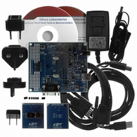
KIT DEVELOPMENT FOR C8051T606
Manufacturer
Silicon Laboratories Inc
Type
MCUr
Datasheets
1.C8051T600EDB.pdf
(188 pages)
2.C8051T606TDB.pdf
(1 pages)
3.C8051T606DK.pdf
(16 pages)
4.C8051T606TDB.pdf
(14 pages)
Specifications of C8051T606DK
Contents
Board, Adapter, Cable, CD, Power Supply
Processor To Be Evaluated
C8051T606x
Interface Type
RS-232, USB
Maximum Operating Temperature
+ 85 C
Minimum Operating Temperature
- 40 C
Operating Supply Voltage
3.3 V
Lead Free Status / RoHS Status
Lead free / RoHS Compliant
For Use With/related Products
C8051T606
Lead Free Status / Rohs Status
Lead free / RoHS Compliant
Other names
336-1666


C8051T60x-DK
7.4. PORT I/O Connector (J8)
Each of the C8051T60x’s I/O pins, as well as VPP, +3VD, GND, and /RST are routed to header J8. This header can
be used to easily connect to any signal on the device. Table 2 defines the pins for header J8.
7.5. Serial Interface (J2)
A RS232 transceiver circuit and DB-9 (J2) connector are provided on the main board to facilitate serial connections
to UART0 on the C8051T60x. The TX and RX signals of UART0 may be connected to the RS-232 transceiver by
installing shorting blocks on header J3. The RTS and CTS lines do not have a direct connection available to the
C8051T60x, due to limited pin resources on the device. However, these two signals have also been routed through
the transceiver, and are available for wiring on-board at test points near the DB-9 connector. The transceiver shifts
the UART signals to RS-232 levels, and connects to the appropriate pins on the DB-9 connector.
7.6. Analog I/O (J6)
Two of the C8051T60x target device’s port pins are connected to the J6 terminal block. Refer to Table 3 for the J6
terminal block connections.
8
J3[1–2]
J3[3–4]
- Install shorting block to connect UART0 RX (P0.5) to transceiver.
- Install shorting block to connect UART0 TX (P0.4) to transceiver.
Table 3. J6 Terminal Block Pin Descriptions
Pin #
1
2
3
4
Table 2. J8 Pin Descriptions
Pin #
10
12
11
1
2
3
4
5
6
7
8
9
+3VD (+3.3 VDC)
Rev. 0.1
GND (Ground)
Description
Description
P0.0/VREF
P0.1/AIN1
/RST
GND
VPP
P0.0
P0.1
P0.2
P0.3
P0.4
P0.5
P0.6
P0.7
VDD
Related parts for C8051T606DK
Image
Part Number
Description
Manufacturer
Datasheet
Request
R

Part Number:
Description:
SMD/C°/SINGLE-ENDED OUTPUT SILICON OSCILLATOR
Manufacturer:
Silicon Laboratories Inc
Part Number:
Description:
Manufacturer:
Silicon Laboratories Inc
Datasheet:
Part Number:
Description:
N/A N/A/SI4010 AES KEYFOB DEMO WITH LCD RX
Manufacturer:
Silicon Laboratories Inc
Datasheet:
Part Number:
Description:
N/A N/A/SI4010 SIMPLIFIED KEY FOB DEMO WITH LED RX
Manufacturer:
Silicon Laboratories Inc
Datasheet:
Part Number:
Description:
N/A/-40 TO 85 OC/EZLINK MODULE; F930/4432 HIGH BAND (REV E/B1)
Manufacturer:
Silicon Laboratories Inc
Part Number:
Description:
EZLink Module; F930/4432 Low Band (rev e/B1)
Manufacturer:
Silicon Laboratories Inc
Part Number:
Description:
I°/4460 10 DBM RADIO TEST CARD 434 MHZ
Manufacturer:
Silicon Laboratories Inc
Part Number:
Description:
I°/4461 14 DBM RADIO TEST CARD 868 MHZ
Manufacturer:
Silicon Laboratories Inc
Part Number:
Description:
I°/4463 20 DBM RFSWITCH RADIO TEST CARD 460 MHZ
Manufacturer:
Silicon Laboratories Inc
Part Number:
Description:
I°/4463 20 DBM RADIO TEST CARD 868 MHZ
Manufacturer:
Silicon Laboratories Inc
Part Number:
Description:
I°/4463 27 DBM RADIO TEST CARD 868 MHZ
Manufacturer:
Silicon Laboratories Inc
Part Number:
Description:
I°/4463 SKYWORKS 30 DBM RADIO TEST CARD 915 MHZ
Manufacturer:
Silicon Laboratories Inc
Part Number:
Description:
N/A N/A/-40 TO 85 OC/4463 RFMD 30 DBM RADIO TEST CARD 915 MHZ
Manufacturer:
Silicon Laboratories Inc
Part Number:
Description:
I°/4463 20 DBM RADIO TEST CARD 169 MHZ
Manufacturer:
Silicon Laboratories Inc