C8051F005DK Silicon Laboratories Inc, C8051F005DK Datasheet - Page 169
C8051F005DK
Manufacturer Part Number
C8051F005DK
Description
DEV KIT FOR F005/006/007
Manufacturer
Silicon Laboratories Inc
Type
MCUr
Datasheet
1.C8051F005-TB.pdf
(171 pages)
Specifications of C8051F005DK
Contents
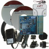
Evaluation Board, Power Supply, USB Cables, Adapter and Documentation
Processor To Be Evaluated
C8051F01x
Interface Type
USB
Silicon Manufacturer
Silicon Labs
Core Architecture
8051
Silicon Core Number
C8051F005
Silicon Family Name
C8051F00x
Lead Free Status / RoHS Status
Contains lead / RoHS non-compliant
For Use With/related Products
Silicon Laboratories C8051 F005/006/007
Lead Free Status / Rohs Status
Lead free / RoHS Compliant
Other names
336-1188
Available stocks
Company
Part Number
Manufacturer
Quantity
Price
Company:

Part Number:
C8051F005DK
Manufacturer:
SiliconL
Quantity:
1


169
C8051F000/1/2/5/6/7
C8051F010/1/2/5/6/7
DATA7
This register is used to read or write data to the Flash memory across the JTAG interface.
Bits9-2: DATA7-0: Flash Data Byte.
Bit1:
Bit0:
This register controls the Flash read timing circuit and the prescaler required to generate the correct
timing for Flash operations.
Bit7:
Bit6:
Bits5-4: UNUSED. Read = 00b, Write = don’t care.
Bits3-0: FLSCL3-0: Flash Prescaler Control Bits.
Bit9
FOSE
Bit7
FAIL: Flash Fail Bit.
0:
1:
0:
1:
0: Flash read strobe is a full clock-cycle wide.
1: Flash read strobe is 50nsec.
0: The Flash output enable and sense amplifier enable are on only when needed to read the
1: The Flash output enable and sense amplifier enable are always on. This can be used to
The FLSCL3-0 bits control the prescaler used to generate timing signals for Flash
operations. Its value should be written before any Flash operations are initiated. The value
written should be the smallest integer for which:
Where f
disallowed when FLSCL[3:0] = 1111b.
FBUSY: Flash Busy Bit.
FOSE: Flash One-Shot Enable Bit.
FRAE: Flash Read Always Bit.
DATA6
Bit8
Flash memory.
limit the variations in digital supply current due to switching the sense amplifiers, thereby
reducing digitally induced noise.
FRAE
Bit6
Previous Flash memory operation was successful.
Previous Flash memory operation failed. Usually indicates the associated memory
location was locked.
Flash interface logic is not busy.
Flash interface logic is processing a request. Reads or writes while FBUSY = 1 will
not initiate another operation
SYSCLK
FLSCL[3:0] > log
DATA5
Figure 21.5. FLASHDAT: JTAG Flash Data Register
Figure 21.6. FLASHSCL: JTAG Flash Scale Register
Bit7
is the system clock frequency. All Flash read/write/erase operations are
Bit5
-
DATA4
Bit6
2
(f
SYSCLK
DATA3
Bit4
Bit5
-
/ 50kHz)
Rev. 1.7
DATA2
FLSCL3
Bit4
Bit3
DATA1
Bit3
FLSCL2
Bit2
DATA0
Bit2
FLSCL1
Bit1
FAIL
Bit1
FLSCL0
FBUSY
Bit0
Bit0
Reset Value
Reset Value
0000000000
00000000
Related parts for C8051F005DK
Image
Part Number
Description
Manufacturer
Datasheet
Request
R

Part Number:
Description:
SMD/C°/SINGLE-ENDED OUTPUT SILICON OSCILLATOR
Manufacturer:
Silicon Laboratories Inc
Part Number:
Description:
Manufacturer:
Silicon Laboratories Inc
Datasheet:
Part Number:
Description:
N/A N/A/SI4010 AES KEYFOB DEMO WITH LCD RX
Manufacturer:
Silicon Laboratories Inc
Datasheet:
Part Number:
Description:
N/A N/A/SI4010 SIMPLIFIED KEY FOB DEMO WITH LED RX
Manufacturer:
Silicon Laboratories Inc
Datasheet:
Part Number:
Description:
N/A/-40 TO 85 OC/EZLINK MODULE; F930/4432 HIGH BAND (REV E/B1)
Manufacturer:
Silicon Laboratories Inc
Part Number:
Description:
EZLink Module; F930/4432 Low Band (rev e/B1)
Manufacturer:
Silicon Laboratories Inc
Part Number:
Description:
I°/4460 10 DBM RADIO TEST CARD 434 MHZ
Manufacturer:
Silicon Laboratories Inc
Part Number:
Description:
I°/4461 14 DBM RADIO TEST CARD 868 MHZ
Manufacturer:
Silicon Laboratories Inc
Part Number:
Description:
I°/4463 20 DBM RFSWITCH RADIO TEST CARD 460 MHZ
Manufacturer:
Silicon Laboratories Inc
Part Number:
Description:
I°/4463 20 DBM RADIO TEST CARD 868 MHZ
Manufacturer:
Silicon Laboratories Inc
Part Number:
Description:
I°/4463 27 DBM RADIO TEST CARD 868 MHZ
Manufacturer:
Silicon Laboratories Inc
Part Number:
Description:
I°/4463 SKYWORKS 30 DBM RADIO TEST CARD 915 MHZ
Manufacturer:
Silicon Laboratories Inc
Part Number:
Description:
N/A N/A/-40 TO 85 OC/4463 RFMD 30 DBM RADIO TEST CARD 915 MHZ
Manufacturer:
Silicon Laboratories Inc
Part Number:
Description:
I°/4463 20 DBM RADIO TEST CARD 169 MHZ
Manufacturer:
Silicon Laboratories Inc