CY3684 Cypress Semiconductor Corp, CY3684 Datasheet - Page 11
CY3684
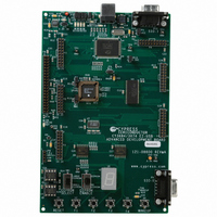
Manufacturer Part Number
CY3684
Description
KIT DEVELOPMENT EZ-USB FX2LP
Manufacturer
Cypress Semiconductor Corp
Series
EZ-USB FXr
Type
MCUr
Datasheet
1.CY3684.pdf
(28 pages)
Specifications of CY3684
Contents
2 Boards, Cables, CD
Silicon Manufacturer
Cypress
Application Sub Type
USB
Kit Application Type
Interface
Silicon Core Number
CY7C68013A-128AXC
Features
FX2LP Development Kit
Silicon Family Name
EZ-USB FX2LP
Rohs Compliant
No
Lead Free Status / RoHS Status
Contains lead / RoHS non-compliant
For Use With/related Products
CY7C68013A-128AC, CY7C64713-128AC
Lead Free Status / RoHS Status
Contains lead / RoHS non-compliant
Other names
428-1677
CY3684
Q2204408
CY3684
Q2204408


4.3 Jumpers
4.4 EEPROM Select & Enable Switches SW1 and SW2
SW1 selects between two socketed EEPROMS, one strapped to address 000 (U6), and the other
strapped to address 001(U5).
SW2 enables or disables the EEPROM selected by SW1.
The EZ-USB chip has various start-up modes, which depend on the existence of an EEPROM
connected to its SCL and SDA lines. Switches SW1 and SW2 allow the EEPROMS to be “discon-
nected” from FX2, or to be connected using one of two EEPROMS installed in sockets U5 and U6.
The EZ-USB chip contains two I
The boot load controller operates when EZ-USB comes out of reset, and the 8051 controller oper-
ates under firmware control once the 8051 is running, permitting the 8051 to access general- pur-
pose I
of SW1 and SW2 in accommodating the various boot load mechanisms.
The EZ-USB boot loader accommodates two EEPROM types, in “Small” and “Large” versions, as
shown by Table 2.
EZ-USB Development Board
Jumper
JP1
JP2
JP3
JP5
JP6
JP7
JP8
JP9
2
C devices connected to the SCL and SDA lines. The discussion below deals with the roles
Connects 3.3 volt
power to the EZ-USB
chip.
Powers the on-board
3.3 volt regulator from
USB Vbus pin
Connects four GAL
pins to LEDS D2, D3,
D4, D5
3.3 Volt Power
Memory map selec-
tion
Wakeup2 Pin
I2C bus test points
Function
Table 1. EZ-USB Development Board Jumpers
Default
2
C controllers, a “boot load” controller, and an 8051 controller.
(1-2)
(1-2)
(1-2)
(3-4)
(5-6)
(7-8)
(1-2)
OUT
(1-2)
OUT
(1-2)
n/a
IN
IN
IN
IN
To operate the board in self-powered mode, remove JP2 and
supply 4-5V to JP2-1, and GND to a ground pin (TP1 is a
convenient GND point).
U2, the on-board GAL, contains code to use the four LEDs
as software settable indicators. If you wish to (a) use the
GAL pins for something else, which requires re-programming
the GAL or (b) wire the general purpose indicators D2-D5 to
other parts of the board, first remove the appropriate shorting
plug(s).
Supplies 3.3 volt power to the board. It may be removed and
replaced with ammeter probes in series to measure board
current.
These jumpers select one of four memory maps for U3, the
external 128 Kilobyte RAM. See the Memory Map section
for details.
Inserting a shorting plug into JP8 connects an on-board RC
network (R42,C43) to the secondary remote wakeup pin
WU2. This R-C network can be used to test periodic remote
wakeup firmware when this dual-purpose pin (it defaults to
PA3) is programmed as WU2.
The I2C bus SCL and SDA lines may be monitored or exter-
nally connected using JP9.
Notes
Page -7
Related parts for CY3684
Image
Part Number
Description
Manufacturer
Datasheet
Request
R

Part Number:
Description:
Manufacturer:
Cypress Semiconductor Corp
Datasheet:
Part Number:
Description:
Manufacturer:
Cypress Semiconductor Corp
Datasheet:
Part Number:
Description:
Manufacturer:
Cypress Semiconductor Corp
Datasheet:
Part Number:
Description:
Manufacturer:
Cypress Semiconductor Corp
Datasheet:
Part Number:
Description:
Manufacturer:
Cypress Semiconductor Corp
Datasheet: