CY3684 Cypress Semiconductor Corp, CY3684 Datasheet - Page 10
CY3684
Manufacturer Part Number
CY3684
Description
KIT DEVELOPMENT EZ-USB FX2LP
Manufacturer
Cypress Semiconductor Corp
Series
EZ-USB FXr
Type
MCUr
Datasheet
1.CY3684.pdf
(28 pages)
Specifications of CY3684
Contents
2 Boards, Cables, CD
Silicon Manufacturer
Cypress
Application Sub Type
USB
Kit Application Type
Interface
Silicon Core Number
CY7C68013A-128AXC
Features
FX2LP Development Kit
Silicon Family Name
EZ-USB FX2LP
Rohs Compliant
No
Lead Free Status / RoHS Status
Contains lead / RoHS non-compliant
For Use With/related Products
CY7C68013A-128AC, CY7C64713-128AC
Lead Free Status / RoHS Status
Contains lead / RoHS non-compliant
Other names
428-1677
CY3684
Q2204408
CY3684
Q2204408


EZ-USB Development Kit Manual - Getting Started
4.0
EZ-USB Advanced Development Board
4.1 Introduction
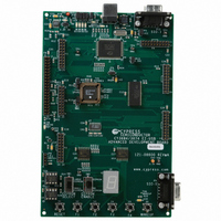
The Cypress Semiconductor EZ-USB Advanced Development Board provides a compact evalua-
tion and design vehicle for the EZ-USB family. The board provides expansion and interface sig-
nals on six 20-pin headers. A mating prototype board allows quick construction and testing of
USB designs. All ICs on the board operate at 3.3 volts. The board may be powered from the
USB connector or an external power supply.
The EZ-USB Advanced Development Board is supplied as part of the Cypress Semiconductor EZ-
USB Development Kit, which includes an evaluation version of Cypress-customized software
development tools from Keil Software Inc. The Keil 8051 assembler, C compiler and debugger
work in concert with the development board to provide a complete code development environ-
ment. An 8051 debug monitor is typically loaded into development board expansion RAM to leave
the internal RAM free for code development. The evaluation version of the Keil tools that ships
with the DVK has several restrictions that make it inappropriate for real-world development. Most
significantly, it limits the compiled object size to 4 Kbytes. The full retail version allows code of any
size.
4.2 Schematic Summary
This description should be read while referring to the EZ-USB FX2LP Development Board Sche-
matic and the FX2LP Development Board Assembly drawing. Both drawings are attached to the
end of this document and are available in PDF format in the DVK hardware directory. With the
exception of the EZ-USB chip, the development boards in the FX2LP and FX1 DVKs are identical
and will be referred to generically as the EZ-USB Development Board in the following sections.
U1 is either EZ-USB FX2LP (CY7C68013A-128AC) or FX1 (CY7C64713-128AC). This is the full-
function EZ-USB chip which brings out the 8051 address and data buses for external memory
expansion. U2, a re-programmable GAL, provides RAM enable signals for four jumper-selectable
memory maps. U3 is a 128 Kilobyte RAM, used for external 8051 memory expansion. Only 64K of
this memory is addressed by the 8051; the A16 pin is connected to a pull-up resistor that may be
attached to a GAL output to provide bank switching options.
U4 is a 3.3V, 500 milliamp voltage regulator. U5 and U6 are socketed EEPROMS, used for EZ-
USB initialization and 8051 general purpose access. U7 converts the 3.3V 8051 serial port signals
to bipolar RS-232 levels. U8 and U10 are Philips PCF8574 IO expanders, which attach to the EZ-
2
USB I
C bus and provide 8 general purpose input-output pins. U10 reads the four push-button
switches S2-S5, and U11 drives the seven-segment readout U9.
Six 20-pin headers, P1-P6, provide interface signals to the plug-in proto-typing board supplied in
this kit, as well as serving as connection points for HP(Agilent) logic analyzer pods. P8 contains a
subset of signals from P1-P6 on a connector that is pinned out for connection to a ‘straight-
through’ ATA cable.
Two slide switches, SW1 and SW2, control the connection and selection of the two socketed
EEPROMS at U5 and U6.
Page -6
EZ-USB Development Kit Manual - Getting Started Rev 1.0
Related parts for CY3684
Image
Part Number
Description
Manufacturer
Datasheet
Request
R

Part Number:
Description:
Manufacturer:
Cypress Semiconductor Corp
Datasheet:
Part Number:
Description:
Manufacturer:
Cypress Semiconductor Corp
Datasheet:
Part Number:
Description:
Manufacturer:
Cypress Semiconductor Corp
Datasheet:
Part Number:
Description:
Manufacturer:
Cypress Semiconductor Corp
Datasheet:
Part Number:
Description:
Manufacturer:
Cypress Semiconductor Corp
Datasheet: