XE8000EV104 Semtech, XE8000EV104 Datasheet - Page 113
XE8000EV104
Manufacturer Part Number
XE8000EV104
Description
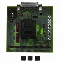
EVAL BOARD FOR XE8805AMI028LF
Manufacturer
Semtech
Type
MCUr
Specifications of XE8000EV104
Contents
Fully Assembled Evaluation Board
For Use With/related Products
XE88LC05AMI028
Lead Free Status / RoHS Status
Contains lead / RoHS non-compliant


As an example, consider the system where: GD
5V. In this case, the noise contribution V
V
Considering a 0.2V (rms) maximum signal amplitude, the signal-to-noise ratio is 90dB.
Noise can also be reduced by implementing a software filter. By making an average on a number of subsequent
measurements, the apparent noise is reduced the square root of the number of measurement used to make the
average.
16.8.5
Gain error is defined as the amount of deviation between the ideal transfer function (theoretical equation Eq. 18)
and the measured transfer function (with the offset error removed).
The actual gain of the different stages can vary depending on the fabrication tolerances of the different elements.
Although these tolerances are specified to a maximum of ±3%, they will be most of the time around ±0.5%.
Moreover, the tolerances between the different stages are not correlated and the probability to get the maximal
error in the same direction in all stages is very low. Finally, these gain errors can be calibrated by the software at
the same time with the gain errors of the sensor for instance.
Figure 16-19 shows gain error drift vs. temperature for different PGA gains. The curves are expressed in % of Full-
Scale Range (FSR) normalized to 25°C.
© Semtech 2006
N,IN
= 6.4µV (rms) at the input of the acquisition chain, or, equivalently, 0.85 LSB at the output of the ADC.
Gain Error and Offset Error
Figure 16-17. ADC noise (PGA1, 2 & 3 bypassed, OSR=512,N
Figure 16-18. (a) Simple noise model for PGAs and ADC
V
PGA1
GD1
N,IN
PGA1
V
GD1
80
60
40
20
0
N1
and (b) total input referred noise
N1
-5
of PGA1 is dominant over that of PGA2. Using equation Eq. 21, we get:
-4
Output Code Deviation From Mean Value [LSB]
PGA2
GD2
2
-3
= 10 (GD
PGA2
GD2
-2
V
N2
16-27
(a)
(b)
-1
1
= 1; PGA3 bypassed), OSR = 512, N
0
PGA3
GD3
PGA3
GD3
1
V
2
N3
3
ADC
ADC
4
f
f
S
S
5
ELCONV
XE8805/05A
=2)
ELCONV
www.semtech.com
= 2, V
REF
=
Related parts for XE8000EV104
Image
Part Number
Description
Manufacturer
Datasheet
Request
R

Part Number:
Description:
EVALUATION BOARD
Manufacturer:
Semtech
Datasheet:
Part Number:
Description:
EVALUATION BOARD
Manufacturer:
Semtech
Datasheet:
Part Number:
Description:
VOLTAGE SUPPRESSOR, TRANSIENT SEMTECH
Manufacturer:
Semtech
Datasheet:

Part Number:
Description:
HIGH VOLTAGE CAPACITORS MONOLITHIC CERAMIC TYPE
Manufacturer:
Semtech Corporation
Datasheet:
Part Number:
Description:
EZ1084CM5.0 AMP POSITIVE VOLTAGE REGULATOR
Manufacturer:
Semtech Corporation
Datasheet:
Part Number:
Description:
3.0 AMP LOW DROPOUT POSITIVE VOLTAGE REGULATORS
Manufacturer:
Semtech Corporation
Datasheet:
Part Number:
Description:
Manufacturer:
Semtech Corporation
Datasheet:
Part Number:
Description:
RailClamp Low Capacitance TVS Diode Array
Manufacturer:
Semtech Corporation
Datasheet:
Part Number:
Description:
Manufacturer:
Semtech Corporation
Datasheet:
Part Number:
Description:
Manufacturer:
Semtech Corporation
Datasheet:
Part Number:
Description:
Manufacturer:
Semtech Corporation
Datasheet:
Part Number:
Description:
Manufacturer:
Semtech Corporation
Datasheet: