DM164120-2 Microchip Technology, DM164120-2 Datasheet - Page 24
DM164120-2
Manufacturer Part Number
DM164120-2
Description
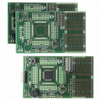
BOARD DEMO PICKIT 2 44PIN
Manufacturer
Microchip Technology
Type
MCUr
Specifications of DM164120-2
Contents
3 Boards (1 Populated, 2 Bare)
Processor To Be Evaluated
PIC16F
Silicon Manufacturer
Microchip
Kit Contents
PIC16F Device, 2 PCB Boards
Features
Small Surface Mount Prototype Area, Two Bare PCB Boards
Development Tool Type
Hardware - Daughter Card
Rohs Compliant
Yes
Lead Free Status / RoHS Status
Lead free / RoHS Compliant
For Use With/related Products
PIC16F887
Lead Free Status / Rohs Status
Lead free / RoHS Compliant
Available stocks
Company
Part Number
Manufacturer
Quantity
Price
Company:

Part Number:
DM164120-2
Manufacturer:
Microchip Technology
Quantity:
135


44-Pin Demo Board User’s Guide
DS41296B-page 20
3.2.4.1
The ADCON1 register sets the justification of the 10-bit result in the 16-bit result read
through registers ADRESL and ADRESH. Setting the result to Left Justified means the
8 Most Significant bits and read from ADRESH and the 2 Least Significant bits are read
from bits 7 and 6 of ADRESL. ADCON1 also sets the voltage reference sources V
and
which the result will be maximum (1023). We select the PIC16F887 V
voltages respectively.
REGISTER 3-1:
3.2.4.2
ADCON0 controls the ADC operation. Bit 0 turns on the ADC module and bit 1 starts a
conversion. Bits <7:6> select the ratio between the processor clock and conversion
speed and bits <5:2> select which channel the ADC will operate on. The ratio between
the processor clock and conversion speed is important because the ADC needs at
least 1.6 μs per bit. Accuracy degrades if the clock speed is too high. As the processor
clock speed increases, an increasingly large divider is necessary to keep the conver-
sion bit speed above 1.6 μs. Four MHz gives the fastest conversion rate above the min-
imum at 8:1 ratio. This results in a conversion speed of 2 μs per bit. Refer to the “T
vs. Device Operating Frequencies” Table in the Analog-to-Digital section of the
PIC16F882/883/884/886/887 Data Sheet (DS41291) for recommended configurations.
For purposes of this lesson, the ADC must be turned on and pointed to channel AN0
on pin RA0.
The ADC needs about 5 μs, after changing channels, to allow the ADC sampling capac-
itor to settle. Finally, we can start the conversion by setting the GO bit in ADCON0. The
bit also serves as the DONE flag. That is, the ADC will clear the same bit when the con-
version is complete. The answer is then available in ADRESH:ADRESL. This lesson
takes the high order 8 bits of the result and copies them to the display LEDs attached
to PORTD.
bit 7
bit 6
bit 5
bit 4
bit 3-0
bit 7
Legend:
R = Readable bit
- n = Value at POR
R/W-0
ADFM
V
REF-.
V
ADCON1
ADCON0
ADFM: A/D Conversion Result Format Selection bit
1 = Right justified
0 = Left justified
Unimplemented: Read as ‘0’
VCFG1: Voltage Reference bit
1 = V
0 = Vss
VCFG0: Voltage Reference bit
1 = V
0 = V
Unimplemented: Read as ‘0’
REF-
U-0
—
REF
REF
DD
is the voltage at which the result will be zero. V
- pin
+ pin
ADCON1: A/D CONTROL REGISTER 1
VCFG1
R/W-0
W = Writable bit
‘1’ = Bit is set
VCFG0
R/W-0
U = Unimplemented bit, read as ‘0’
‘0’ = Bit is cleared
U-0
—
U-0
—
© 2007 Microchip Technology Inc.
REF+
x = Bit is unknown
U-0
—
is the voltage at
SS
and V
bit 0
DD
U-0
—
REF+
AD
Related parts for DM164120-2
Image
Part Number
Description
Manufacturer
Datasheet
Request
R

Part Number:
Description:
SERIES CONNECTION; 16 DIODES
Manufacturer:
Altech Corp.
Datasheet:

Part Number:
Description:
Manufacturer:
Microchip Technology Inc.
Datasheet:
Part Number:
Description:
Manufacturer:
Microchip Technology Inc.
Datasheet:
Part Number:
Description:
Manufacturer:
Microchip Technology Inc.
Datasheet:
Part Number:
Description:
Manufacturer:
Microchip Technology Inc.
Datasheet:
Part Number:
Description:
Manufacturer:
Microchip Technology Inc.
Datasheet:
Part Number:
Description:
Manufacturer:
Microchip Technology Inc.
Datasheet:
Part Number:
Description:
Manufacturer:
Microchip Technology Inc.
Datasheet:
Part Number:
Description:
Manufacturer:
Microchip Technology Inc.
Datasheet: