DM164120-2 Microchip Technology, DM164120-2 Datasheet - Page 14
DM164120-2
Manufacturer Part Number
DM164120-2
Description
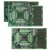
BOARD DEMO PICKIT 2 44PIN
Manufacturer
Microchip Technology
Type
MCUr
Specifications of DM164120-2
Contents
3 Boards (1 Populated, 2 Bare)
Processor To Be Evaluated
PIC16F
Silicon Manufacturer
Microchip
Kit Contents
PIC16F Device, 2 PCB Boards
Features
Small Surface Mount Prototype Area, Two Bare PCB Boards
Development Tool Type
Hardware - Daughter Card
Rohs Compliant
Yes
Lead Free Status / RoHS Status
Lead free / RoHS Compliant
For Use With/related Products
PIC16F887
Lead Free Status / Rohs Status
Lead free / RoHS Compliant
Available stocks
Company
Part Number
Manufacturer
Quantity
Price
Company:

Part Number:
DM164120-2
Manufacturer:
Microchip Technology
Quantity:
135


44-Pin Demo Board User’s Guide
2.3
DS41296B-page 10
INSTRUCTION FORMATS
Data Memory is held in file registers. Instructions referring to file registers use 7 bits,
so only 128 file registers can be addressed. Multiple file registers are arranged into
“banks”. Two bits in the STATUS register, RP0 and RP1, allow accessing different
banks. These two bits effectively become the top two bits of the file register address.
The additional banks may or may not be implemented, depending on the device.
Mid-range devices reserve the first 32 addresses of each bank for Special Function
Registers (SFRs). SFRs are how the program interacts with the peripherals and some
core features. The controls and data registers are memory mapped into the SFR space.
Addresses above 0x20 to the end of each bank are General Purpose Registers
(GPRs), where program variables may be stored.
Some frequently used registers may be accessed from any bank. For example, the
STATUS register is always available no matter which bank is selected via the RP bits.
The last 16 bytes (0x70-0x7F) of the GPRs may also be accessed from any bank.
Program Memory is accessed via a 13-bit Program Counter (PC). The lower 8 bits are
accessible via SFR (PCL), and the upper 5 are at a PCLATH. See the PIC16F88X Data
Sheet’s (DS41291) section on PCL and PCLATH for more details on the PC. PCLATH
becomes important when program memory size exceeds 1k instructions, and also for
the table look-up in Lesson 12.
Mid-range PIC
erwise noted, the lessons in this manual use the Internal Oscillator running at 4 MHz.
Most instructions follow one of three formats: Byte oriented instructions, Bit oriented
instructions and Literal instructions.
Byte instructions contain a 7-bit data address, a destination bit, and a 6-bit op code.
The data address plus the RP0 and RP1 bits create a 9-bit data memory address for
one operand. The other operand is the Working register (called W or WREG). After the
instruction executes, the destination bit (d) specifies whether the result will be stored in
the WREG (‘w’) or back in the original file register (‘f’). For example:
adds the contents of WREG and file register data, with the result going back into data.
Bit instructions operate on a specific bit within a file register. They contain 7 bits of data
address, a 3-bit number and the remaining 4 bits are op code. These instructions may
set or clear a specific bit within a file register. They may also be used to test a specific
bit within a file register. For example:
set the RP0 bit in the STATUS register.
Literal instructions contain the data operand within the instruction. The WREG
becomes the other operand. Calls and GOTO’s use 11 bits as a literal address.
Moves the ASCII value of ‘A’ (0x41) into the WREG.
BSF
MOVLW
ADDWF
data,f
'A'
®
STATUS,RP0
MCUs may be clocked by a number of different devices. Unless oth-
© 2007 Microchip Technology Inc.
Related parts for DM164120-2
Image
Part Number
Description
Manufacturer
Datasheet
Request
R

Part Number:
Description:
SERIES CONNECTION; 16 DIODES
Manufacturer:
Altech Corp.
Datasheet:

Part Number:
Description:
Manufacturer:
Microchip Technology Inc.
Datasheet:
Part Number:
Description:
Manufacturer:
Microchip Technology Inc.
Datasheet:
Part Number:
Description:
Manufacturer:
Microchip Technology Inc.
Datasheet:
Part Number:
Description:
Manufacturer:
Microchip Technology Inc.
Datasheet:
Part Number:
Description:
Manufacturer:
Microchip Technology Inc.
Datasheet:
Part Number:
Description:
Manufacturer:
Microchip Technology Inc.
Datasheet:
Part Number:
Description:
Manufacturer:
Microchip Technology Inc.
Datasheet:
Part Number:
Description:
Manufacturer:
Microchip Technology Inc.
Datasheet: